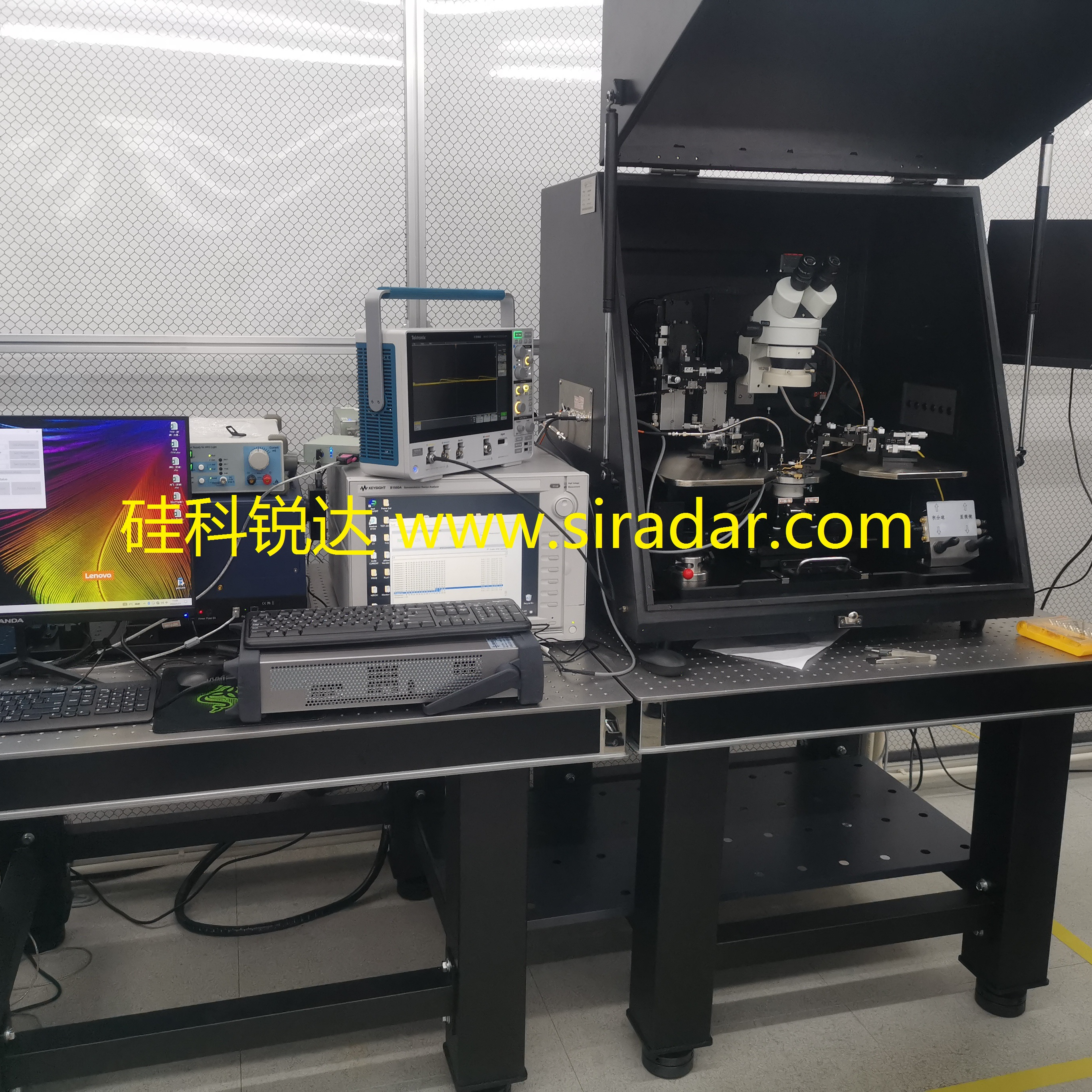


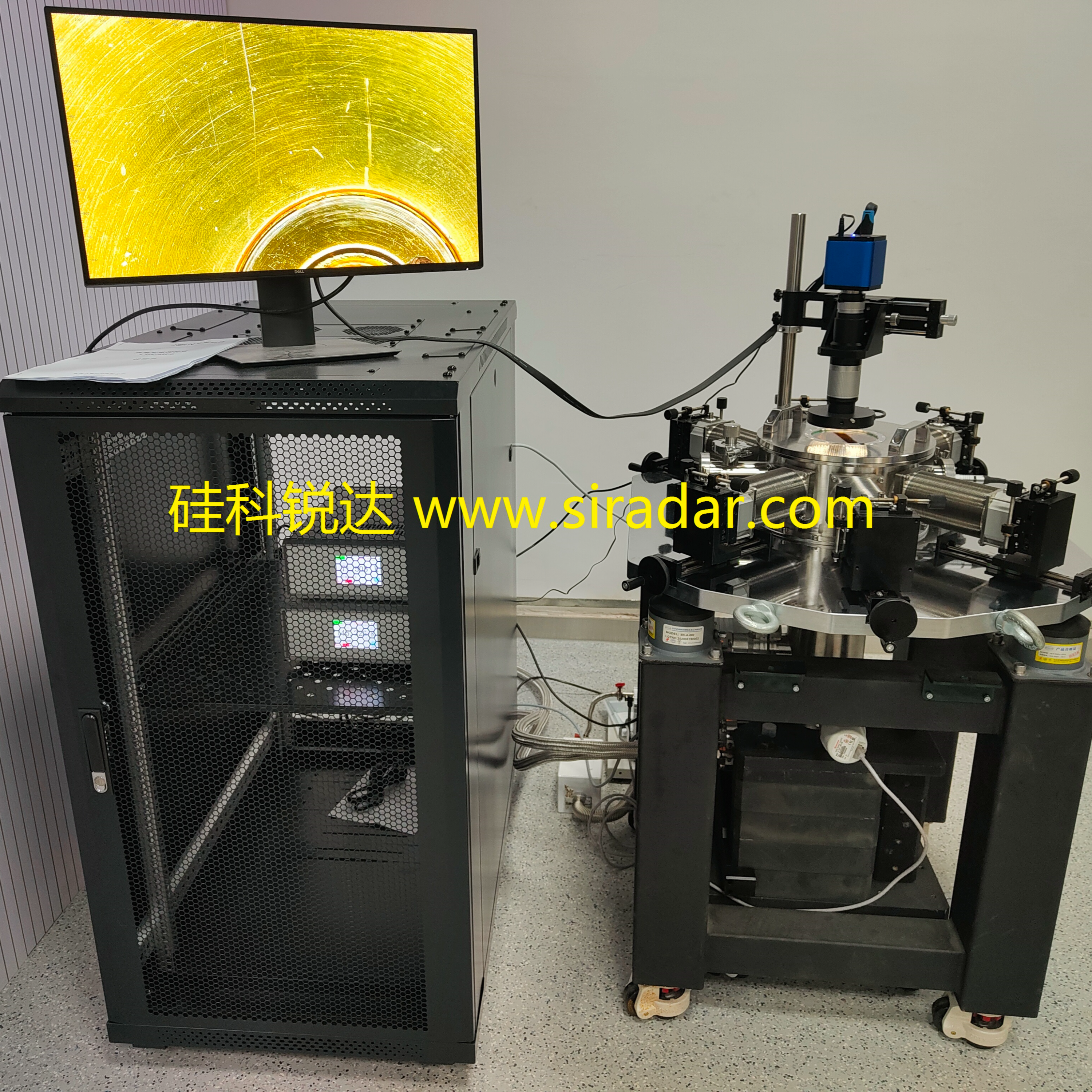


MPS150T 6-inch probe station test solution designed for photonic detector, power semiconductor devices, and RF chip testing.
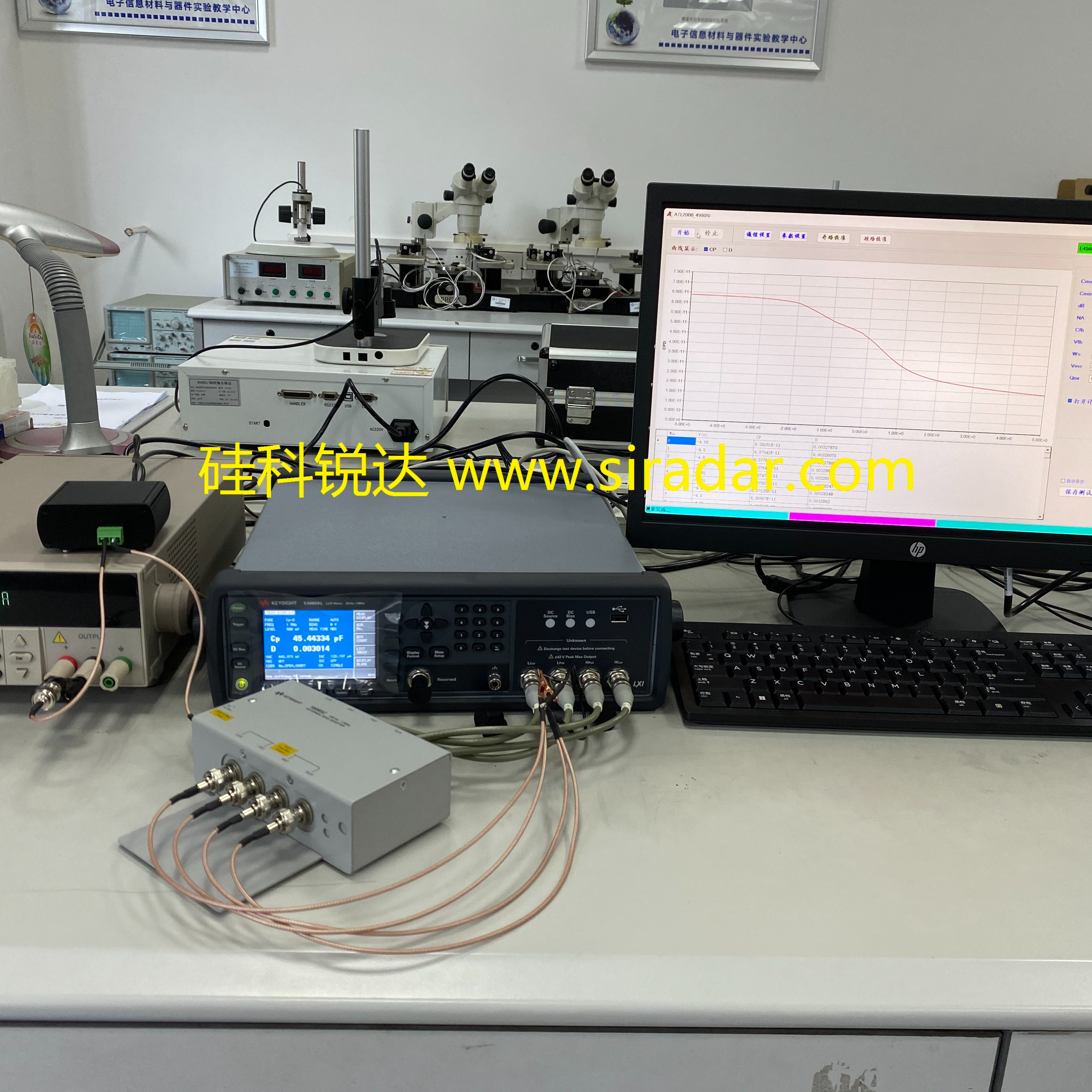
We offer the capability to measure DC IV, CV, RF, and high-voltage high-current. Equipped with a quick guide rail movement of 8 inches, electromagnetic locking, and precision...
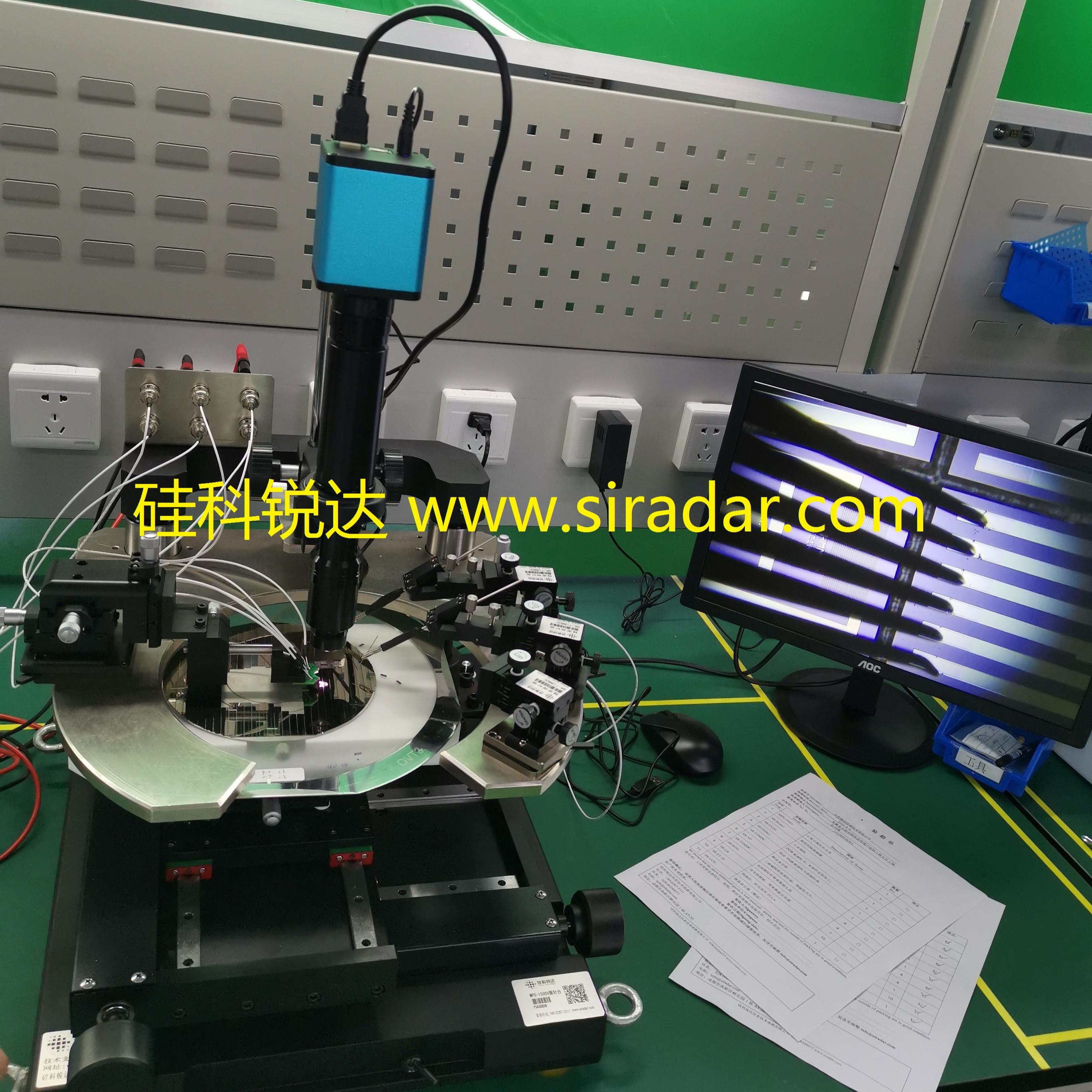
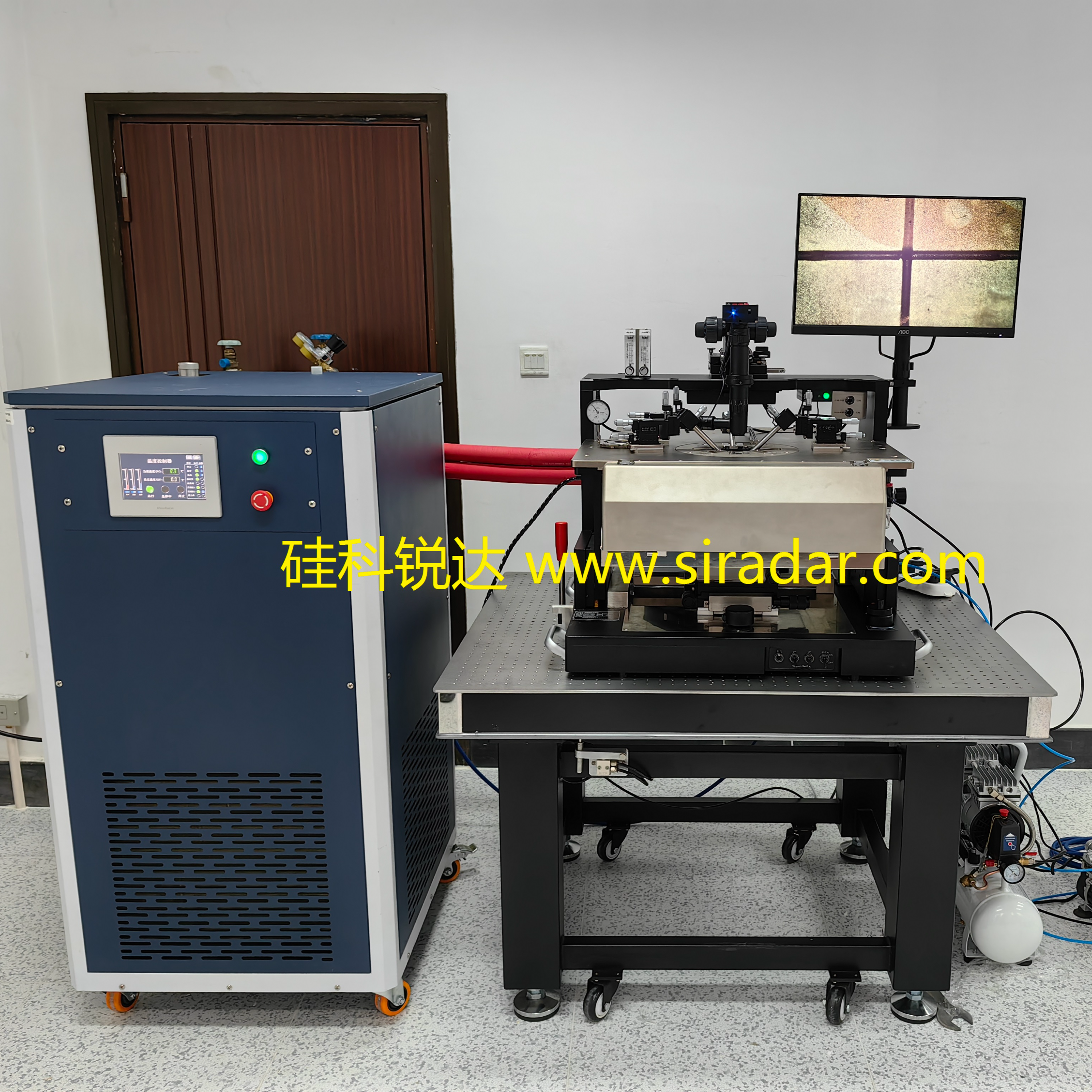
The micrometer precisely locates the Die position of each wafer. The probe station chuck can be heated from room temperature to 200°C for power temperature tests, and the wafer holder is flat.
The surface is gold-plated, ensuring low contact resistance during testing, ultra-thin wafer processing, and power dissipation, while providing low leakage noise.
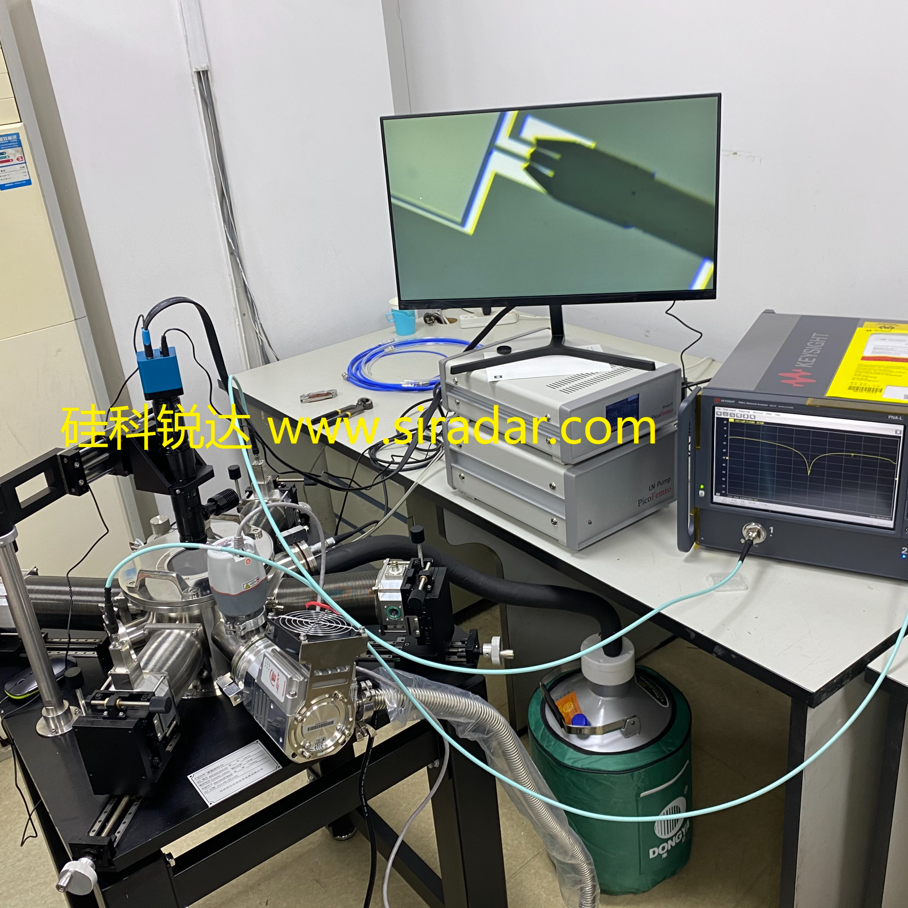
Sound protection <1 pA and light-blocking electromagnetic shielding environment.
Application: Wafer, Chip Testing for Devices (RF, IGBT, GaN, SiC, etc.)
Feature:
Wafer Level Testing Capabilities: DC, Photoelectric, Power Temperature Testing
Wafer Stage Surface: Gold-plated treatment, ensuring the lowest contact resistance between the wafer surface and the stage.
Safe Operation: Interlock mechanisms ensure operator safety during testing.
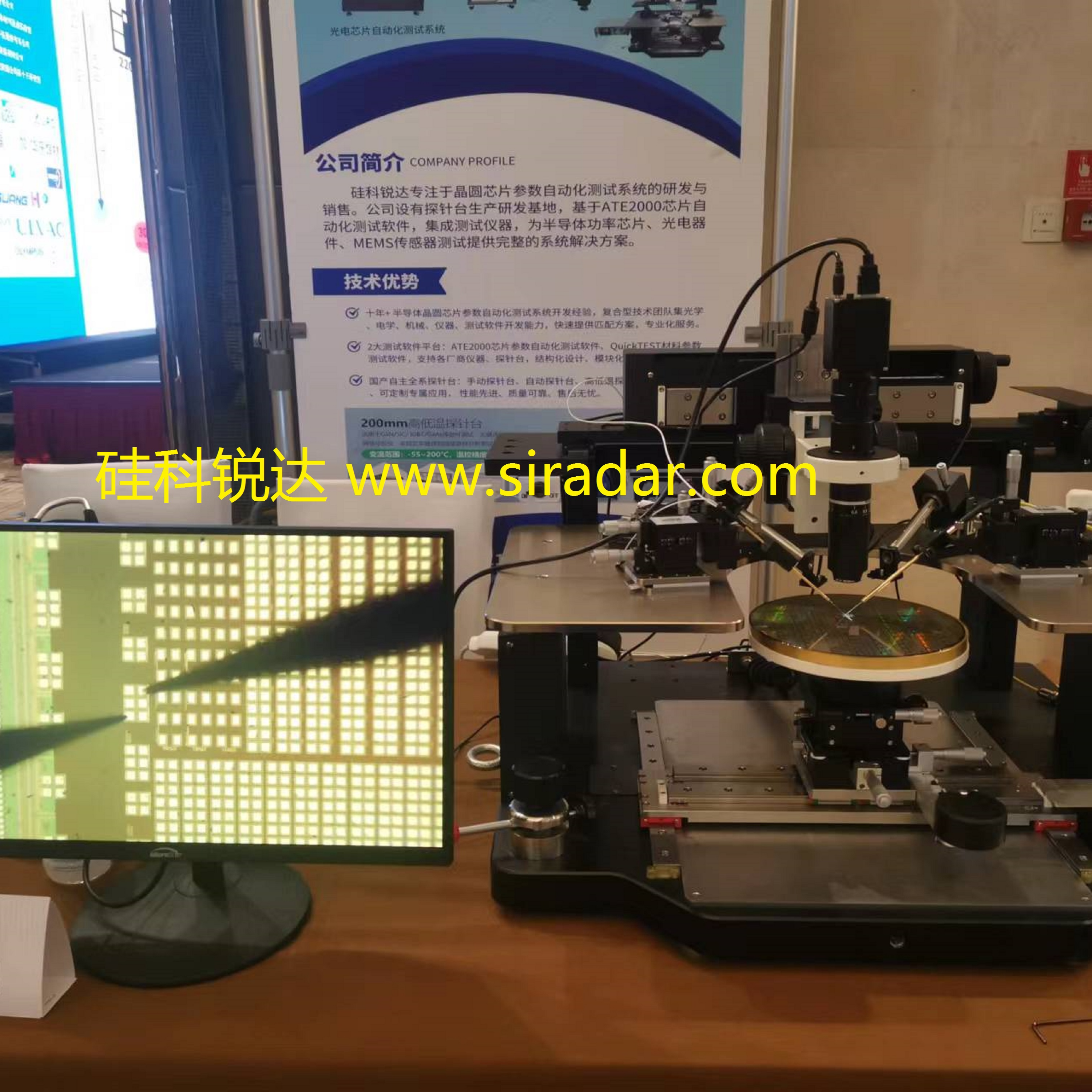
XY Motion: Quick sliding track drive, air floating lock, precise micrometer adjustment
Signal Connection: Signal Transfer Kit combined with Keysight B1505A Analyzer
Test equipment, simply and quickly to set up a test system
Configuration
MPS150T: Probe Station Main Unit
Microscope: Monocular body microscope with lens
Probe: DC Probe, Optical Probe, RF Probe
Electromagnetic Shielding: Custom Electromagnetic Shielding Enclosure
Probe Mount: Precision magnetic suction micrometer probe mount, displacement resolution 1um