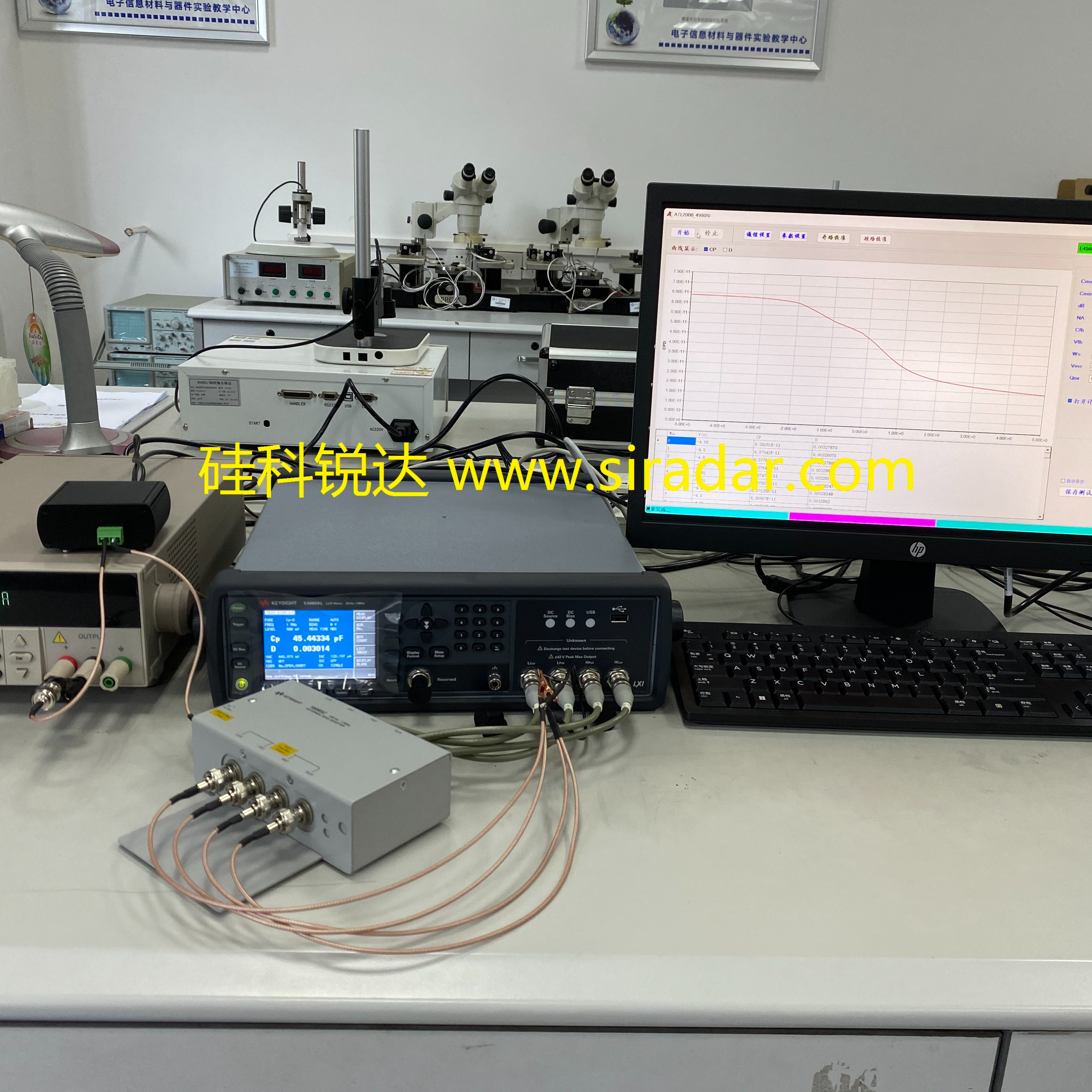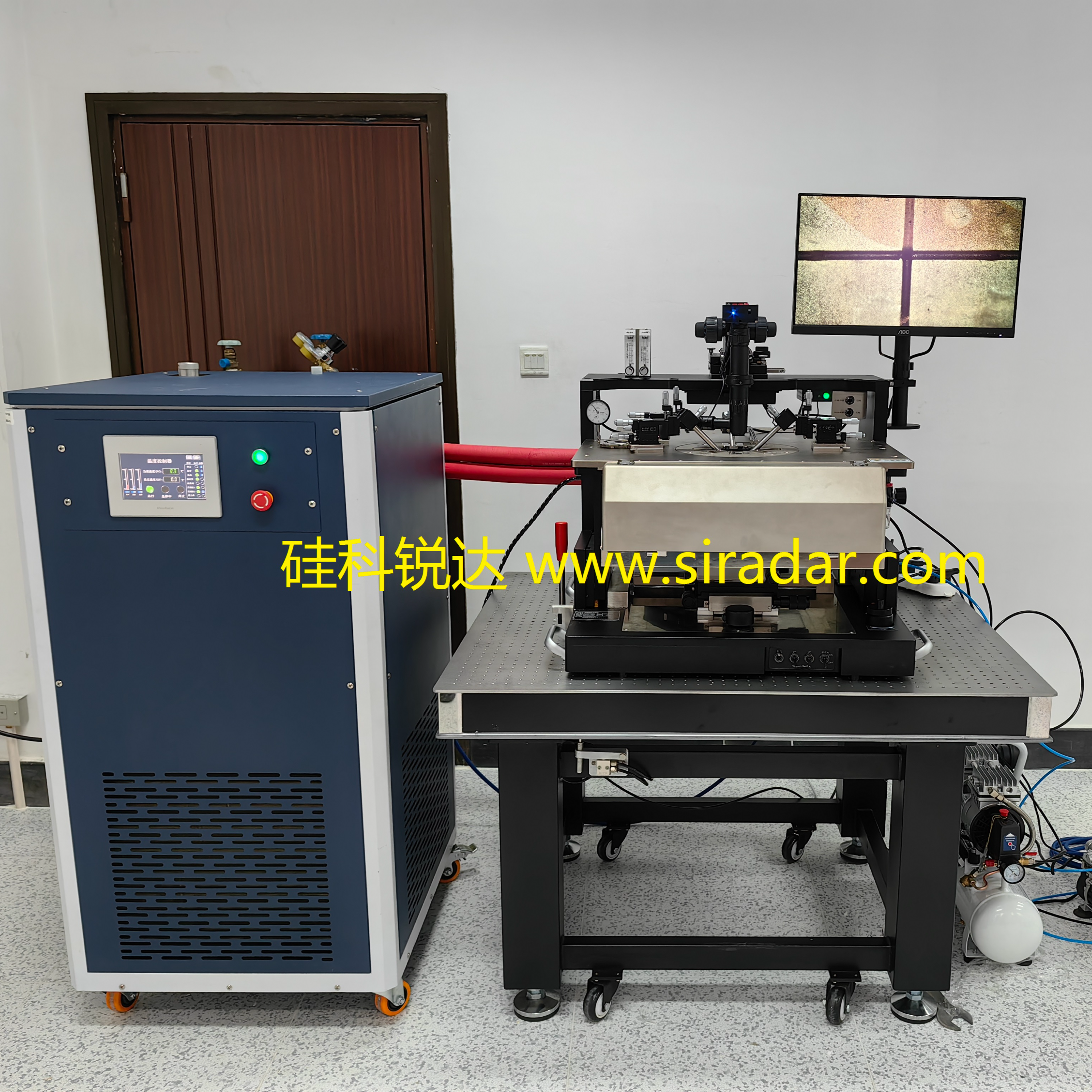
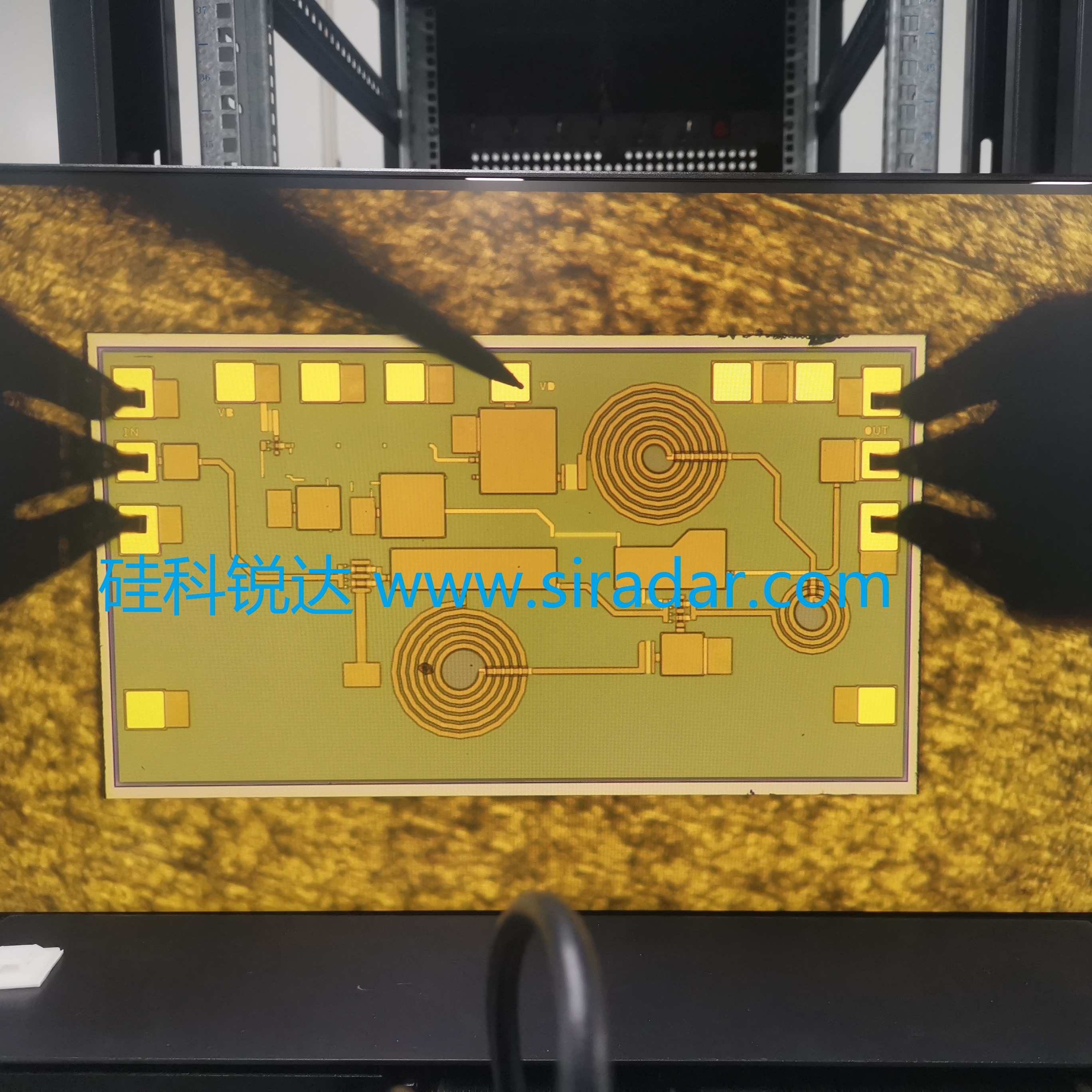
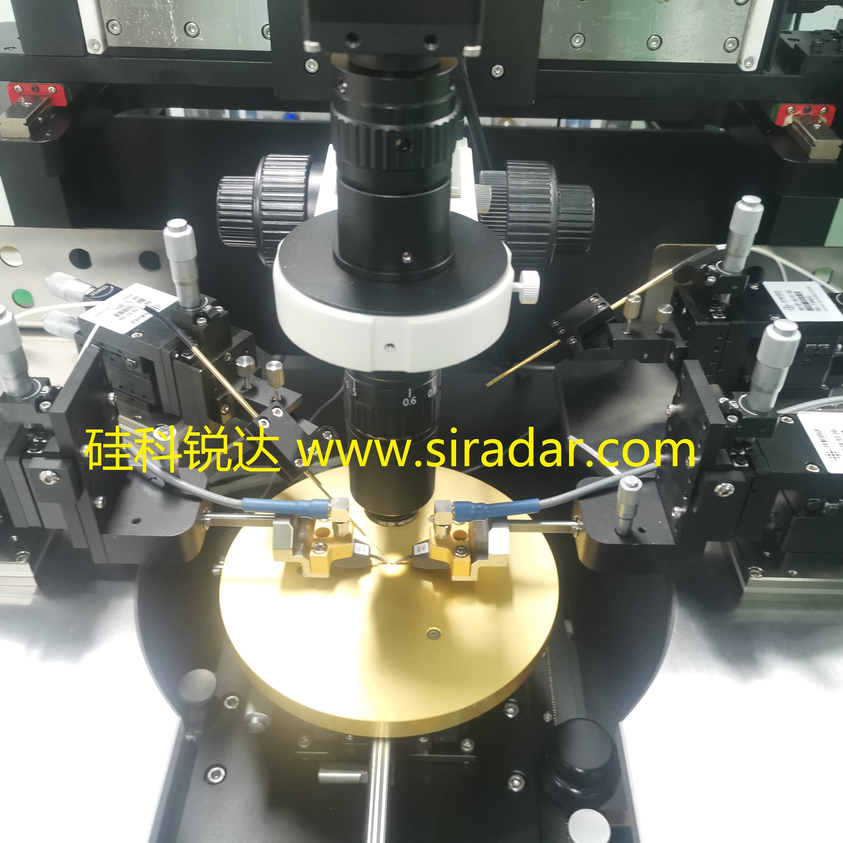


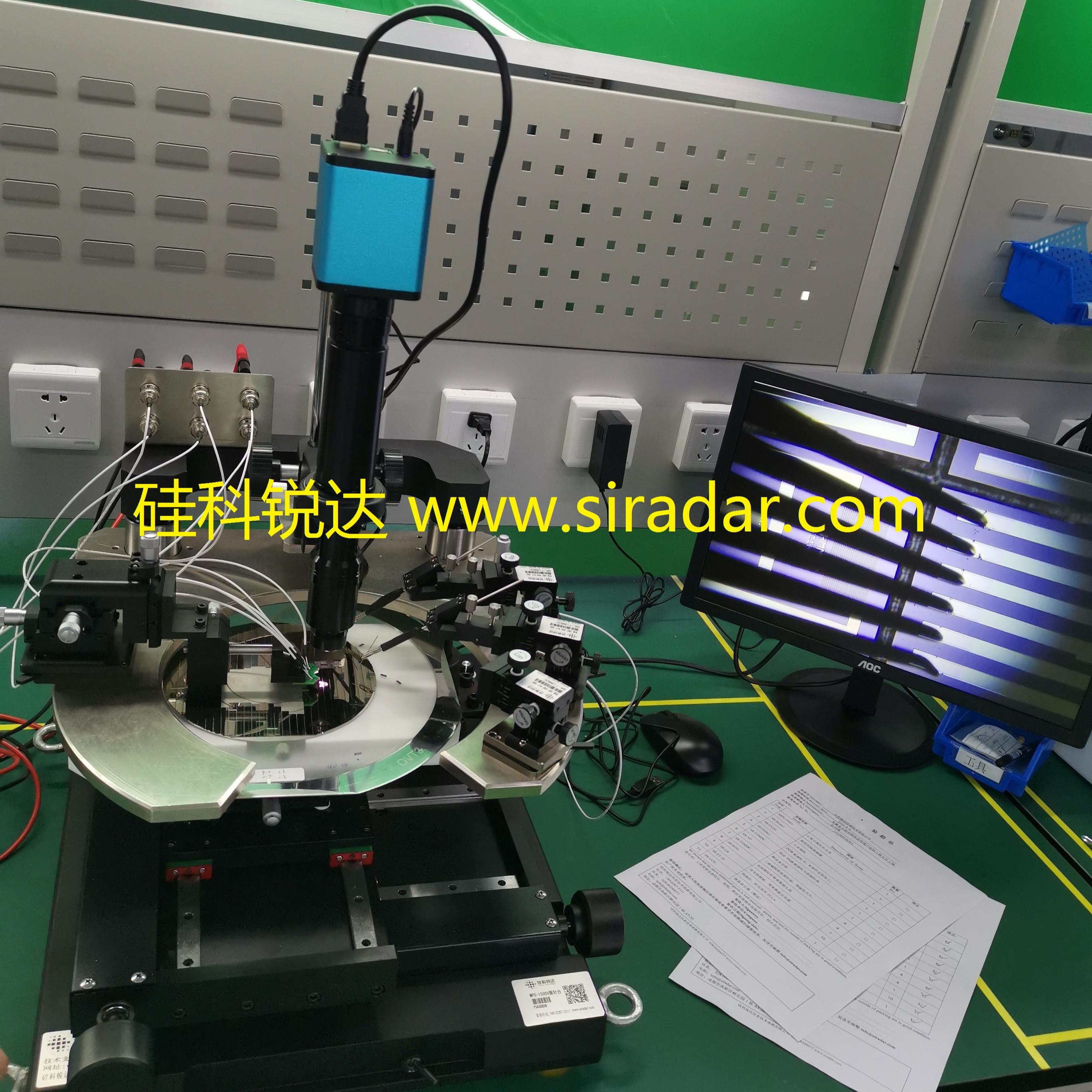
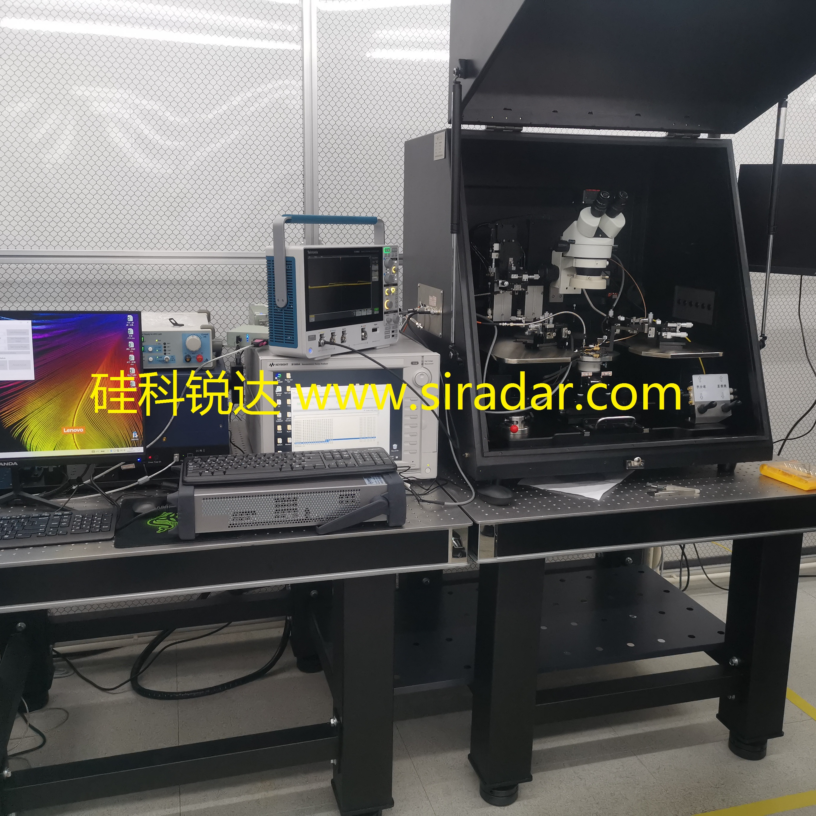
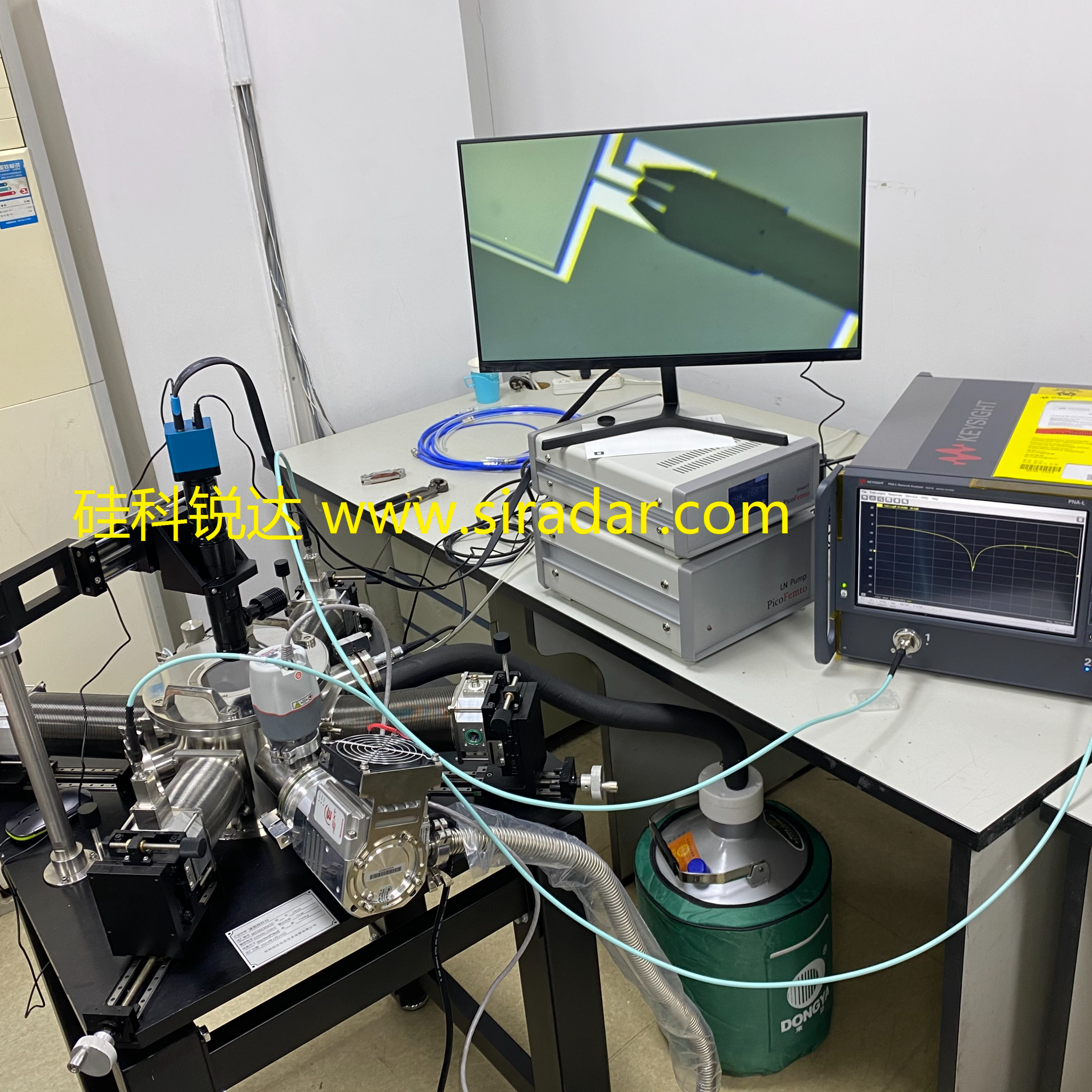
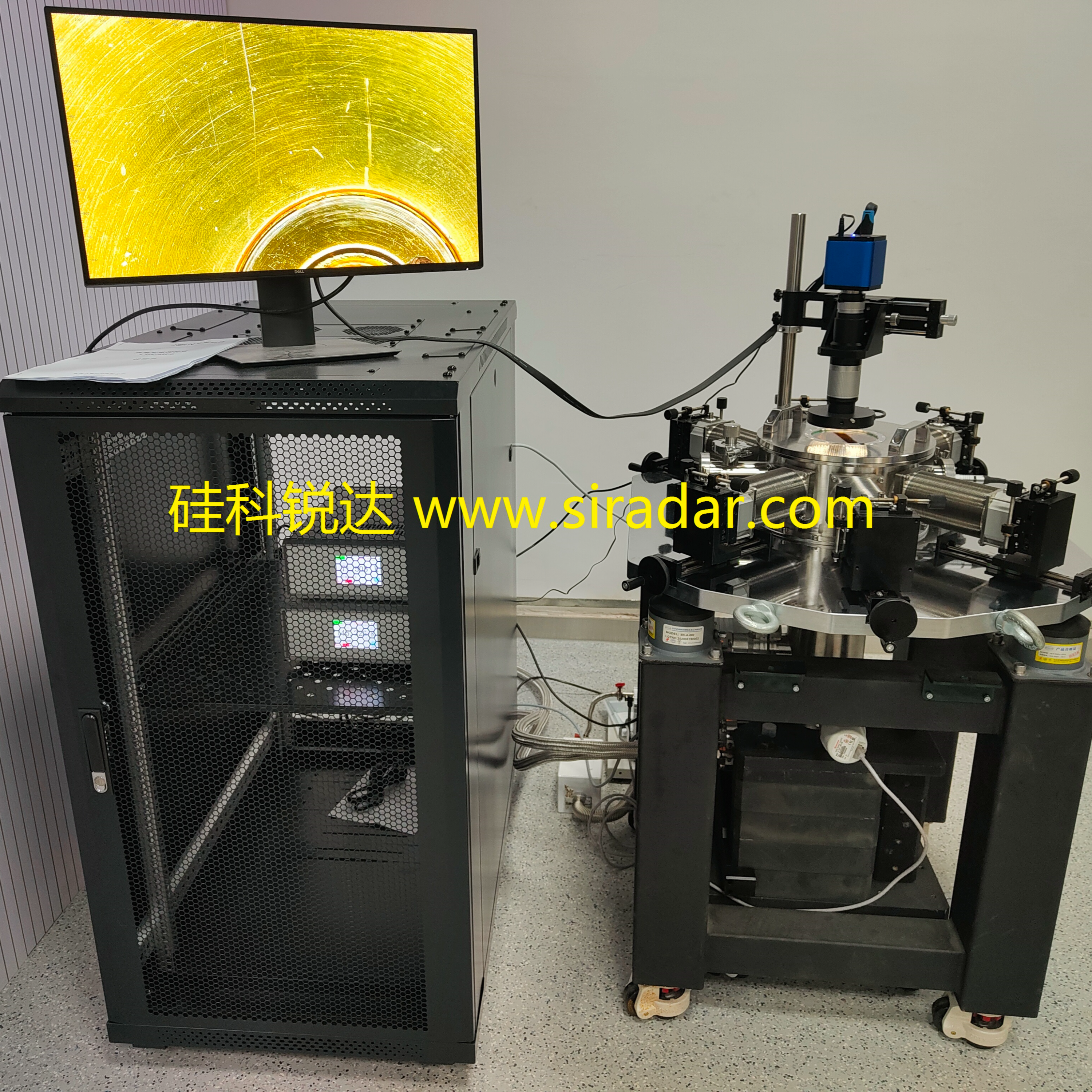


TPS200XT High-Temperature and Low-Temperature Probe Station is an integrated in-situ testing solution designed for wafer testing of power devices, optoelectronic devices, and RF devices. It offers measurement capabilities for DC IV, CV, photoelectric parameters, and RF S-parameters. Combined with a custom micro-sealed chamber and high-temperature/low-temperature control system, it supports high-temperature and low-temperature testing of wafers within a temperature range of -60℃ to 300℃. The probe station's wafer holder platform is made of gold-plated aluminum to ensure low contact resistance during testing, ultra-thin wafer handling, and power dissipation, while also providing low leakage noise protection and shielding environment.
Application:
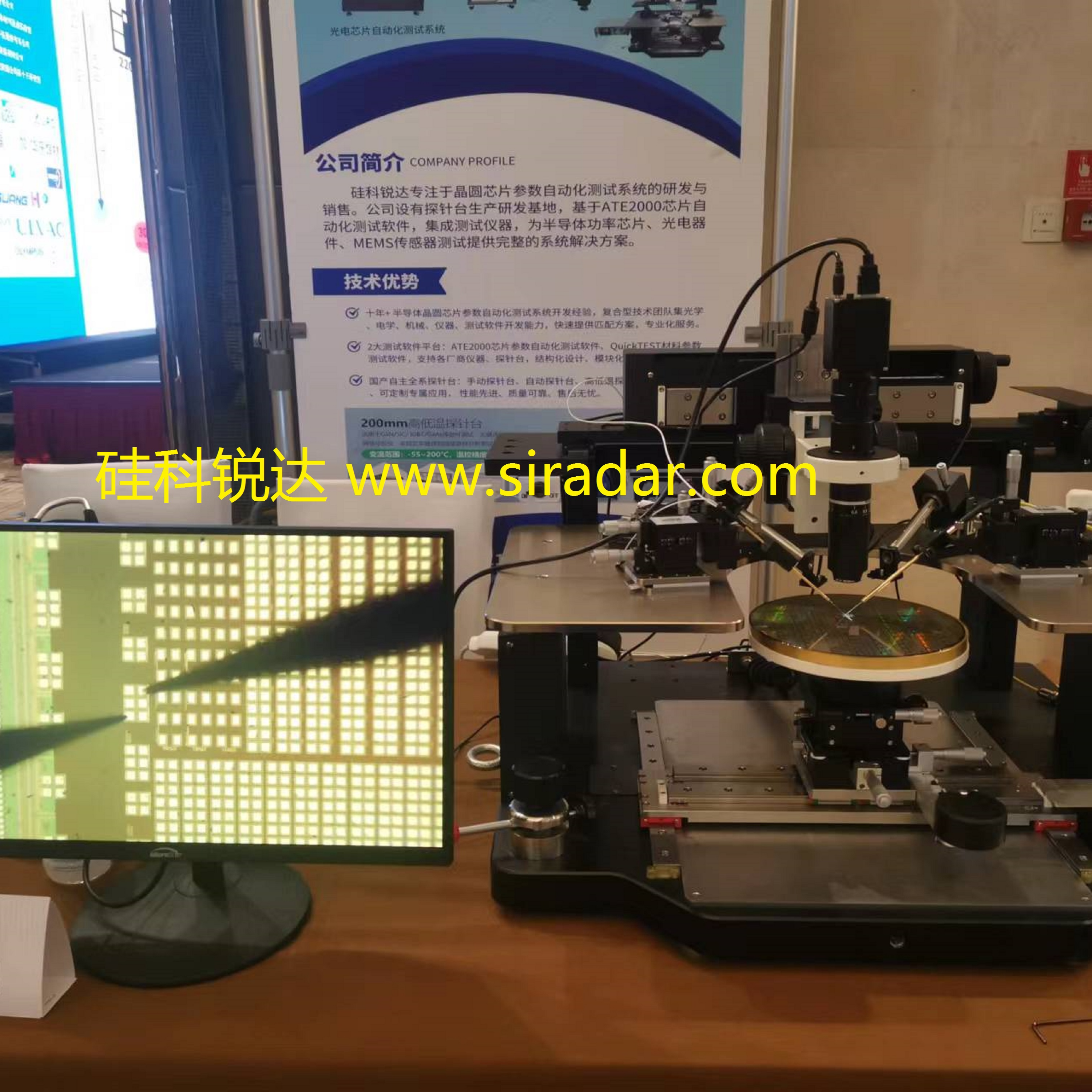
Photodiode/ APD, SiC power semiconductor devices, SAW射频 chips, etc., wafer testing for 8-inch and below diameter
Features
Wafer Level Testing Capabilities: DC, Photoelectric, RF Parameter Testing
Temperature Range: -60℃ to 300℃
Wafer Stage Surface: Special gold plating treatment ensures the lowest wafer surface and
Wafer Stage Contact Resistance
Safety Measures: Utilizing CE-certified safety light curtains, ensuring secure operation.
Grid sensor infrared detection, automatically detects if objects enter the probe station space.
Automatically cuts off high-voltage power supply, forms a locking mechanism, ensuring the safety of the operator.
Upper and lower film method: Drawer-type structure design of the slide plate, film loading and unloading is effortless.
A gentle push or pull allows for manual sheet lifting and lowering.
Signal Connection: The signal transfer kit is compatible with Keysight's analytical testing instruments.
Effortlessly and quickly set up the test system