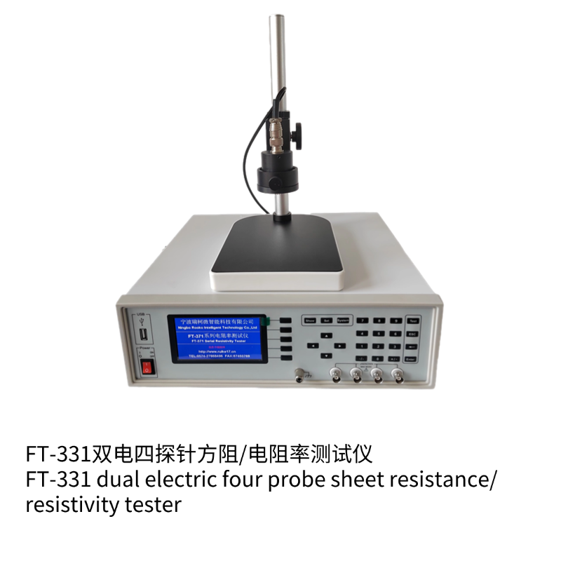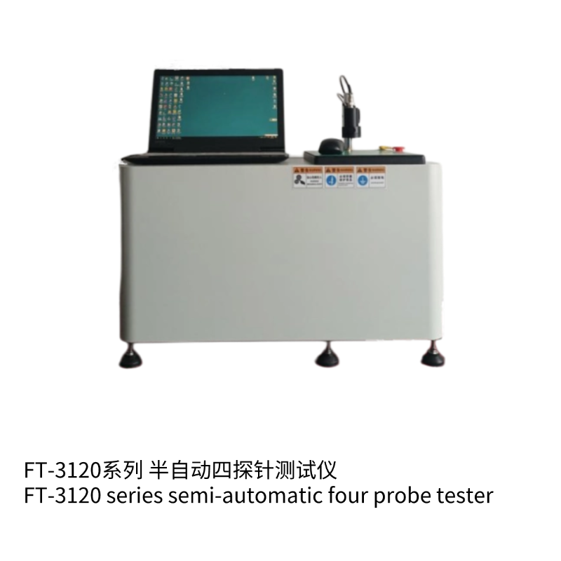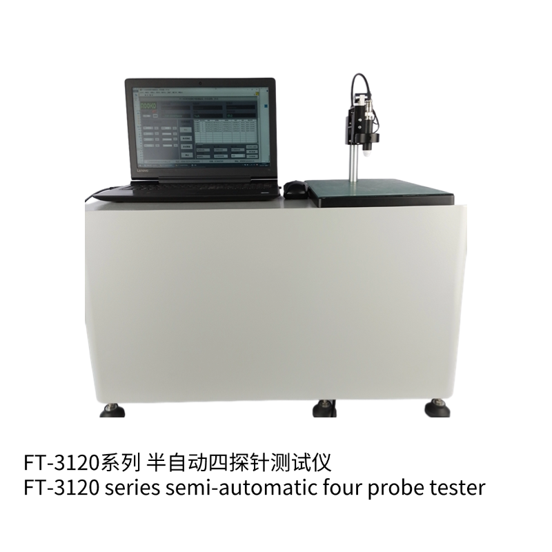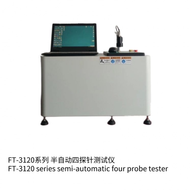
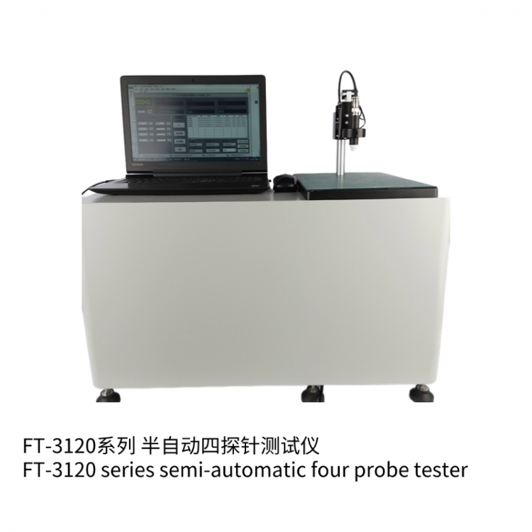


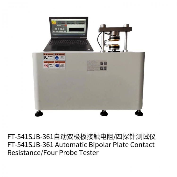
FT-3120B Semi-Automatic Four-Terminal Tester
Function Description: Functionnal description
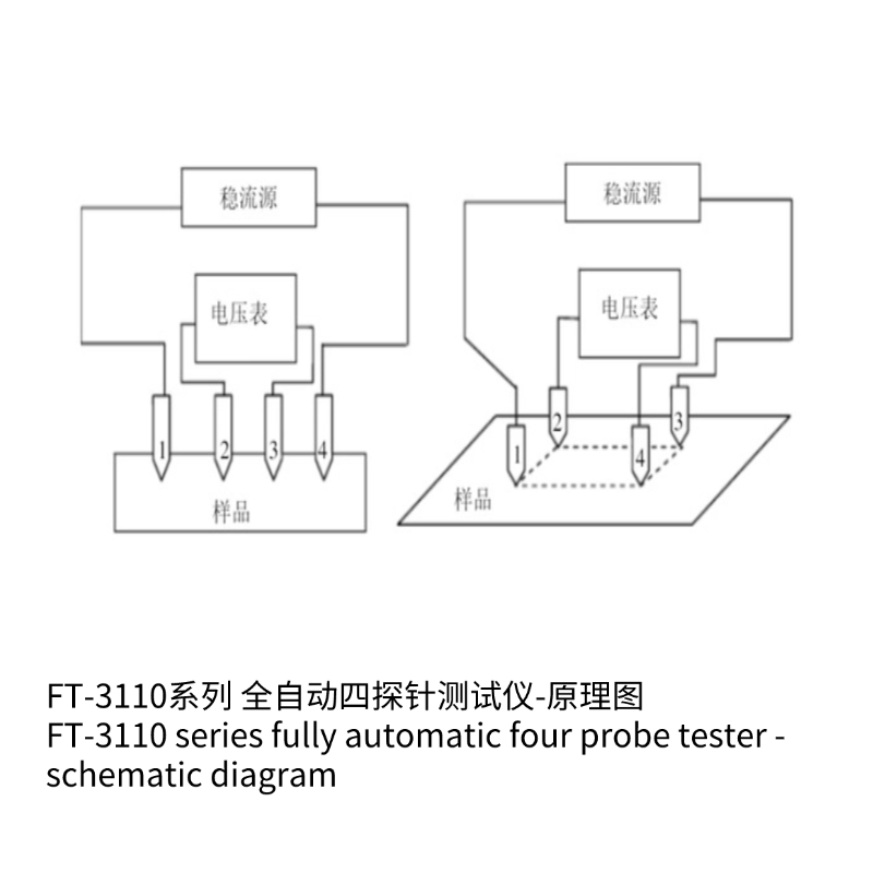
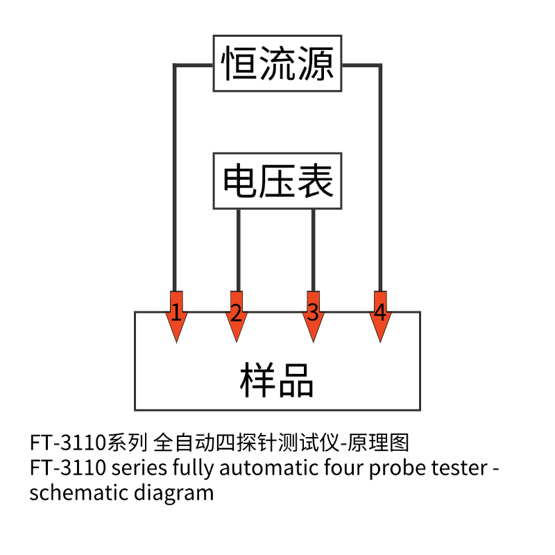
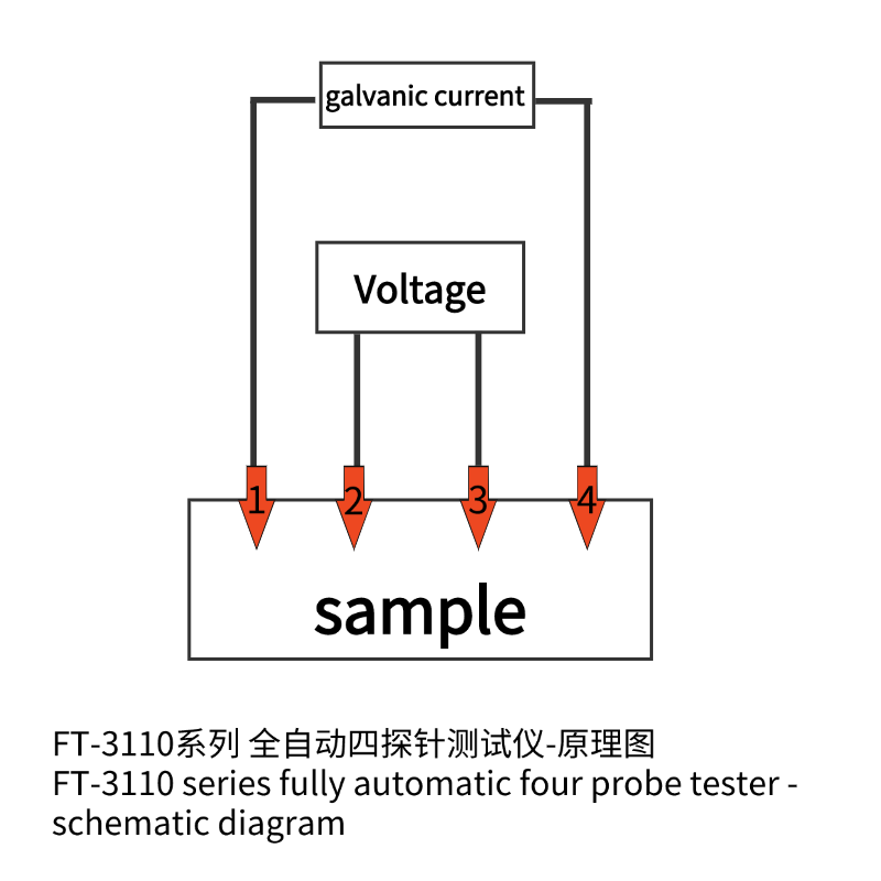
Four-point probe standard testing method, utilizing a stepping system for automatic control of probe contact with the sample, minimizing the impact of human factors on test results; Referenced to A.S.T.M standards; Measures resistance, resistivity, conductivity data, and enables automatic or manual point measurement through PC software data collection and processing; Repeat testing at the same location or multi-point sheet resistance measurement, with data statistical analysis output; Provides standard calibration resistors; Automatic positive/negative current output, automatic positive/negative voltage measurement
Scope of Application
Wafer, amorphous/silicon carbide and conductive film resistivity measurement; selective emitter diffusion wafers; surface passivation wafers; crossbar finger PN junction diffusion wafers; new electrode designs, such as electroplated copper resistance measurement, etc.; semiconductor material analysis, piezoelectric materials, nanomaterials, solar cells, LCDs, OLEDs, touchscreens, etc.
FT-3120B Semi-Automatic Four-Terminal Probe Tester
Technical Specifications
Model and Specifications | FT-3120B |
1.Resistor | 10^-5~2×10^5Ω |
2.Square Resistance | 10^-5~2×10^5Ω/□ |
3.Resistivity | 10^-6~2×10^6Ω-cm |
4.Test Current | 0.1μA.μA.0μA,100µA,1mA,10mA,100mA |
5.Current Accuracy | ±0.1% |
6.Resistance Accuracy | ≤0.3% |
7.PCSoftware Operation | PCSoftware Interface: Resistance, Resistivity, Conductivity, Sheet Resistance, Temperature, Unit Conversion, Current, Voltage, Probe Shape, Probe Spacing, ThicknessData Management Analysis, Large/Low value, mean value, variance, coefficient of variation, sample number, test point count report generation, etc. |
8.Probe Range Selection: | Probe pressure is100-550gBased on sample contact requirements, adjustments are needed. |
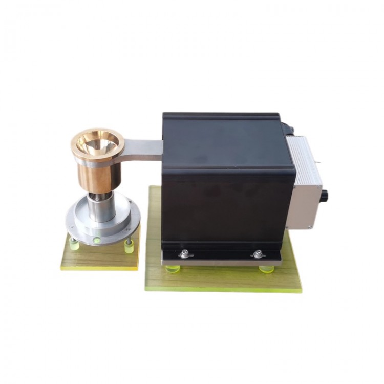
9.ExploreNeedle | Insulation Resistance Between Needles: ≥1000MΩ; Mechanical Hysteresis: ≤0.3% Round head copper-plated gold, tungsten steel material, probe spacing1mm;2mm;3mmOptional accessoriesOther specifications are customizable. |
10.Testable Chip Size Selection | Wafer Size:2-12N/A(6Inch150mm,12Inch300mm); Square Sheets: Up to156mm X 156mm Or125mm X 125mm |
11. Analytical Mode | Automatic or Manual Single-point Mode |
12. Pressure Application Method | Measurement Repeatability: Repeatability ≤3% |
13. Protective Functions | Limited range with pressure protection |
14. Test Environment | Lab environment |
15. Power Supply | AC 220V±10%, 50Hz, Power Consumption: <100W |
16. Selection Items | Computers and printers |