


Product description
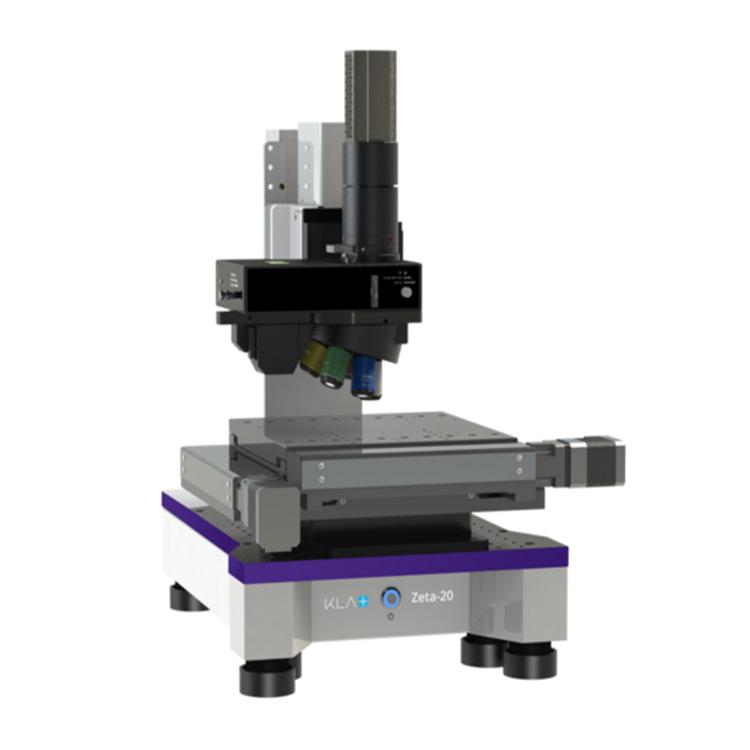
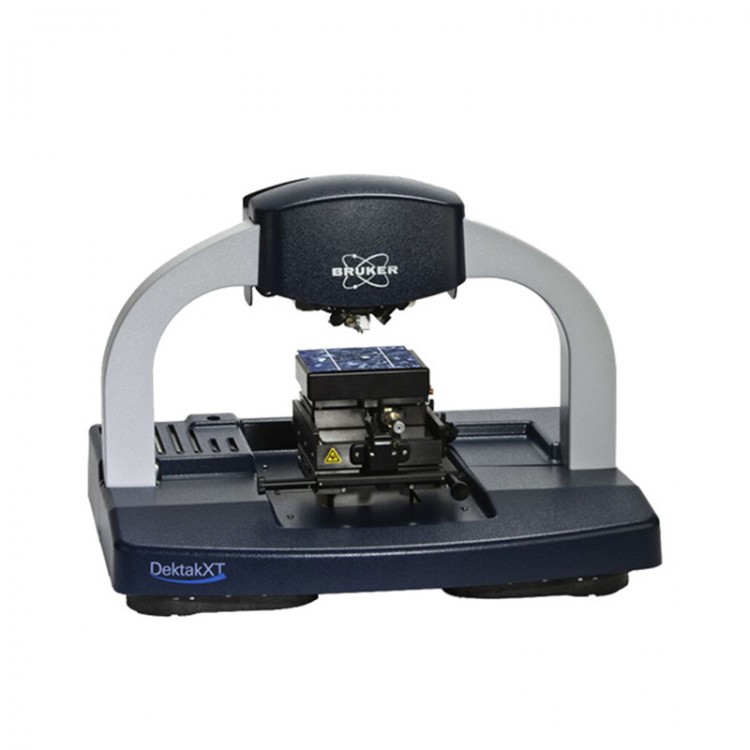
The Zeta-20 desktop optical profilometer is a non-contact 3D surface topography measurement system. This system uses ZDot ™ The patented technology and Multi Mode optical system can measure various types of samples: transparent and opaque, low to high reflectivity, smooth to rough textures, and step heights ranging from nanometers to millimeters.
The configuration of Zeta-20 is flexible and easy to use, and it integrates six different optical measurement techniques. ZDot ™ The measurement mode can simultaneously capture high-resolution 3D data and True Color infinite focus images. Other 3D measurement techniques include white light interferometry, Nomarski interferometric contrast microscopy, and shear interferometry. ZDot or integrated broadband reflectometer can measure the thickness of thin films. Zeta-20 is also a high-end microscope that can be used for sample retesting or automatic defect detection. Zeta-20 is suitable for research and production environments by providing better measurement of step height, roughness, and film thickness, as well as defect detection capabilities.
Main functions
A simple and easy-to-use optical profiler using ZDot and Multi Mode optical components, with a wide range of applications
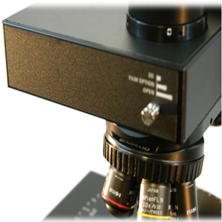
High quality microscope suitable for sample retesting or defect detection
ZDot: Simultaneously collect high-resolution 3D data and True Color infinite focus images
ZXI: White light interferometry measurement technology, suitable for wide area measurement with high z-resolution
ZIC: Interference Contrast, suitable for surfaces with sub nanometer roughness and providing their 3D quantitative data
ZSI: Shear interferometry technology provides high-resolution images in the z-direction
ZFT: Measuring film thickness and reflectivity using an integrated broadband reflectometer
AOI: Automatic optical inspection and quantification of defects on samples
Production capacity: Fully automated measurement achieved through sequencing and pattern recognition
Main applications
Step height: 3D step height ranging from nanometers to millimeters
Texture: Smooth to very rough surface roughness and waviness
Appearance: 3D warping and shape
Stress: 2D thin film stress
Film thickness: 30nm to 100 μ m transparent film thickness
Defect detection: Capture defects larger than 1 μ m
Defect re inspection: Using KLARF files as navigation to measure the 3D surface morphology of defects or the location of cutting defects
industrial applications
Solar energy: Photovoltaic solar cells
Semiconductors and compound semiconductors
Semiconductor WLCSP (wafer level chip level packaging)
Semiconductor FOWLP (Fan Out Wafer Level Packaging)
PCB and flexible PCB
MEMS (Micro Electro Mechanical Systems)
Microfluidic equipment
data storage
Universities, research laboratories, and institutes
More: Please contact us to meet your requirements