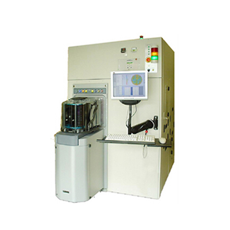


Introduction to Film Stress and Substrate Warpage Testing Equipment
FSM was the first to introduce the laser scanning optilever (Optilever) technology for commercial applications, primarily used in thin film stress and wafer bending measurement. The equipment is frequently utilized in analyzing and solving issues such as how thin film cracks, delamination, bulges, and voids are formed. The FSM128 series of devices is suitable for the research and production of next-generation devices in the semiconductor, III-V, solar, micro-electromechanical systems, data storage, and liquid crystal panel industries.
Rapid & Contactless Laser Scanning
3D View & Outline
Measurable under room temperature & high-temperature conditions
Applicable Wafer Size: 50-300mm (Other sizes available upon request for customization)
Wafers can be transported using mechanical arms.
Key Design Features:
· Multi-purpose
The FSM 128 NT is compatible with wafer sizes ranging from 50 to 200mm without the need to change the wafer sample carrier plate. Other models in the FSM 128 series are primarily designed for different sample sizes. (For example, the FSM128L is capable of measuring wafer samples up to 300mm, while the FSM 128G is specifically designed for measuring panel samples up to 650 x 550mm.)
· Samples are easy to place and retrieve.
An automatically adjustable door mechanism designed for easy placement and retrieval of wafer samples from the sample carrier platform, making multi-wafer measurement effortless.
· Automatic dual-band laser switching
The FSM128 series features automatic laser switching scanning technology. When the sample has poor reflectivity, the system automatically switches to a different wavelength laser for scanning. This allows customers to measure almost all materials including nitride, polyimides, low K, high K, metals, etc.
Certain films do not encounter issues with non-measurability.
· 2-D & 3-D Map
The FSM128 is equipped with a motor-driven rotatable wafer stage, enabling rapid generation of 2-D & 3D Map images. These images help users visualize the curvature and stress distribution across the entire wafer, accurately reflecting areas with process and uniformity issues.
· Film Thickness
The FSM128 can integrate the thickness measurement function for dielectric material films, transforming the device into a powerful desktop unit that can be flexibly used in both R&D and production environments.
Measurement results charts and maps can be easily exported to generate reports in Excel or Word documents.
Primarily used in semiconductor, LED, solar energy, data storage, and LCD panel industries.