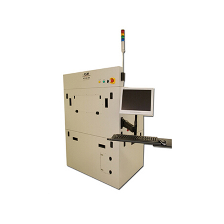


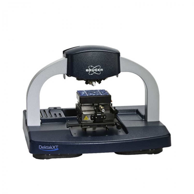
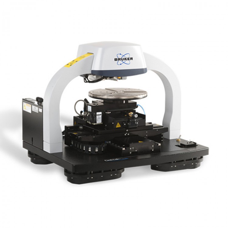
Non-contact thickness measurement for thin wafers post backside lapping and etching, as well as for patterned or raised wafers adhered to blue film or other substrates. Suitable for applications in stacked chips and microelectromechanical systems.
Advantages:
The FSM413 echo probe sensor utilizes infrared (IR) interferometry technology to directly measure substrate thickness changes from thick to thin wafers, as well as overall thickness changes. The single-probe system configuration allows for the measurement of materials transparent to infrared light, such as Si, GaAs, InP, SiC, glass, quartz, and certain polymers. It also measures the substrate thickness of conventional wafers with graphics, tape, bumps, or bonded to substrates. The dual-probe system configuration offers overall wafer thickness measurement (including substrate thickness and graphic height thickness in non-transparent areas). Optional features include measuring groove depth and via depth (including high aspect ratio grooves and vias in microelectromechanical systems). Additionally, film thickness measurement and bump height measurement for microelectromechanical applications are also available as options.
Based on FSM Echoprobe infrared interferometry technology, we offer a non-contact method for measuring chip thickness and depth.
Echoprobe technology utilizes infrared light beams to detect wafers.
Echoprobe is used for measuring polycrystalline silicon, sapphire, and other compound semiconductor materials such as GaAs, InP, GaP, GaN, etc.
Directly measure the wafer substrate cutting surface.
Industry Applications:
Primarily used in chip thickness control during grinding, chip backend packaging, TSV (Through Silicon Via) technology, (MEMS) microelectromechanical systems, and side wall angle measurement.
For the LED industry, suitable for measuring the thickness and TTV of sapphire or silicon carbide wafers.
Other Applications:
· Groove Depth Measurement
· Surface Roughness Measurement
· Film Thickness Measurement
· Epoxy Thickness Measurement