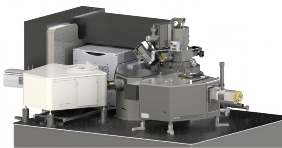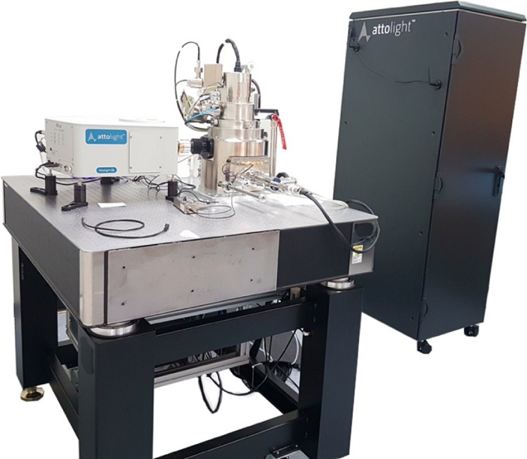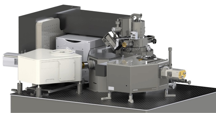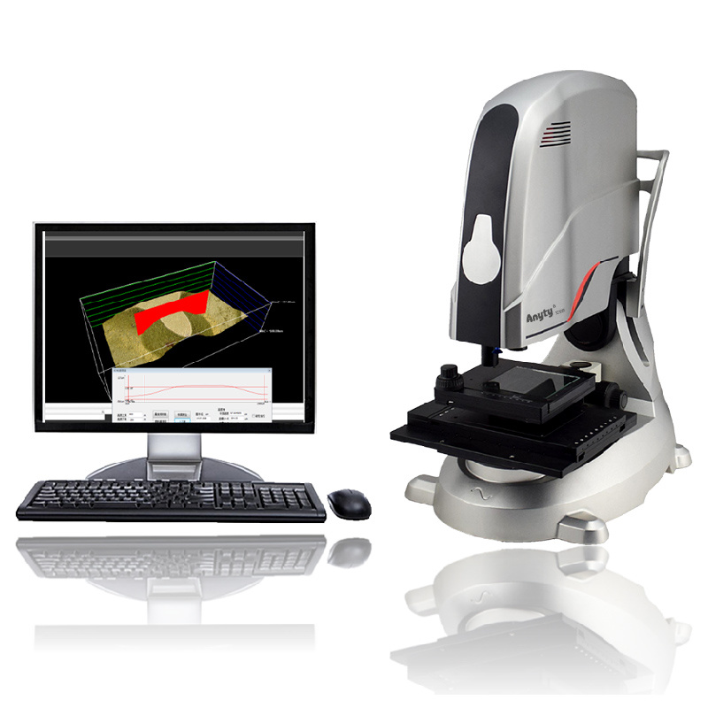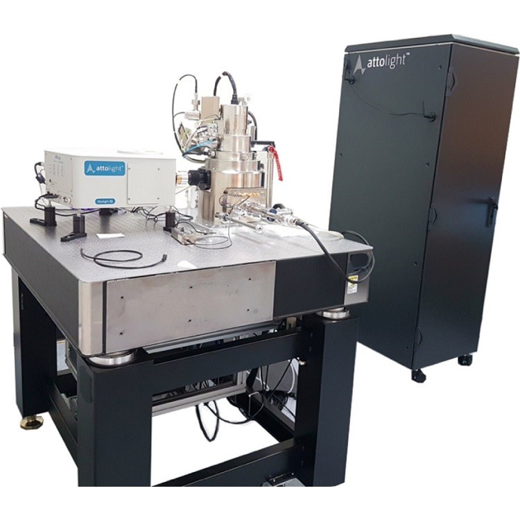


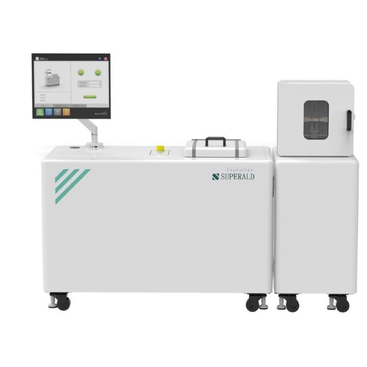
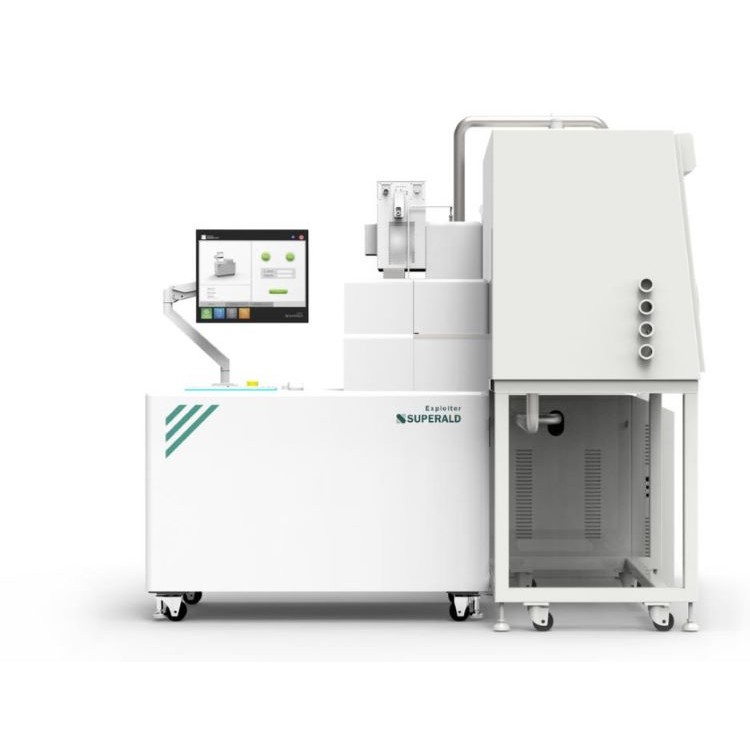
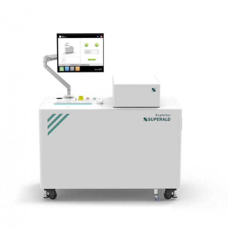

Product Description
Allalin is a nanometer-resolution spectral instrument based on a groundbreaking technology known as quantitative cathodoluminescence. It integrates an optical microscope and a scanning electron microscope (SEM) into a single system. Allalin enables "uncompromising" wide-field rapid scanning while obtaining SEM imaging and high-spectral or full-color CL maps. The system is designed to achieve optimal cathodoluminescence performance without compromising SEM performance: the objectives of the optical microscope and SEM are meticulously integrated to match their focal planes; the optical microscope is processed with sub-micrometer precision, featuring apochromatic, high numerical aperture (N.A. 0.71) detection, and exhibits superior photon collection efficiency in wide fields (up to 300µm). Therefore, quantitative cathodoluminescence, where the workpiece related to the instrument can be fundamentally excluded as a cause of spectral characteristics or contrast, makes the cathodoluminescence signal more reliable.
Allalin is designed for those who require strict technical pathways and rapid access to highly precise spectral information that traditional methods cannot replicate. In semiconductor fault analysis, development, and research, Allalin's spectral measurement capabilities provide unparalleled solutions for fast and reliable defect detection and localization. Verified data types include measurements of dislocation density, material composition fluctuations, strain, dopant types and concentrations; and a wide range of other applications. In scientific research, Allalin can create spectral maps with nanometer resolution, making it the ultimate tool for in-depth understanding of the physical properties of materials at the nanoscale. Allalin offers a comprehensive set of features: a variety of detectors covering the ultraviolet-infrared wavelength range, SE detectors, a stable low-temperature sample stage, and high-sensitivity EBIC (electron beam induced current) detection solutions.
Technical Specifications
| Electro-optical System | – Short skirt hot cathode electron gun – Electron Beam Energy 1keV–10keV – Electron beam spot size: 3nm @ 10kV – Working Distance 3mm – High-sensitivity SE detector – Upgradable to a picosecond pulsed laser electron gun (For more information, please refer to Chronos information) – Probe Current: 30pA to 300nA |
| Optical System | – Field of view up to 300µm – Integrated Light Collection System: 30% of photons emitted from the Lambertian source exit the microscope (constant throughout the field of view) – Colorless achromatic objective from 180nm to 1.6µm – Numerical Aperture: NA 0.71 (f/0.5) |
| Optical detection | – Dispersive Spectrometer, with two imaging outputs (320mm focal length) and a 3-grating turret (Attolight offers a wide range of diffraction gratings to match your application), high-speed CCD camera for UV-Vis light (200 nm – 1100 nm) measurement with electrically adjustable entrance and exit slits, maximum speed >900 spectra/second – InGaAs camera for near-infrared (600 nm–1700 nm) detection with highest speed >180 spectra/second – Full-color detection across a range of 200 nm to 1700 nm using various detectors, with the highest speed over 50 ns per pixel |
| Electron Beam Induced Current (EBIC) | Low-noise EBIC circuit board – Current measurement 100 fA – Gain 10^4 to 10^15 V/A – Maximum bandwidth is 100 kHz |
| Sample Room & Vacuum System | – Oil-free vacuum pump system: Suction ion pumps for electron guns and electron columns, and turbo molecular pumps for the sample chamber – Standard Sample Exchange Time: 20 min – Vacuum door equipped with electronic feedthrough |
| Nano Positioning Platform | – 6 degrees of freedom, capable of moving freely (compatible with low-temperature thermostats) – Travel: 25mm (X,Y), 3mm (Z), 3° Tilt (X,Y), 10° Rotation (Z) – Step: 1 nm – Repetition of 100 nm over the entire travel range – Coordinate system, facilitates precise positioning and movement for jing |
| Low-Temperature Constant Temperature System | Temperature range from 10K to room temperature, with a temperature accuracy of 0.1 K. Digital Temperature Controller Imported from Xian – At 10 K, the drift is less than 300 nm per hour |
| System Control and Monitoring Module | – Concurrently perform CL (hyperspectral or full-spectral imaging), SEM, and EBIC analysis Semi-automatic operation mode – Intuitive touch screen-based graphical user interface (GUI) for quick sample location and movement, as well as real-time data display to check measurement status – Maximum image resolution is 4K, with the highest spectral resolution at 512×512 pixels, and the minimum beam dwell time is 50 ns per pixel. |
| Data Analysis | - Attolight offers robust analysis and solutions. For more information, refer to the separate Attomap manual. Tool configuration and CL data are saved simultaneously for the ease of reproducing the tool configuration. – Easily access password-protected measurement data online Export in open data formats, providing flexibility for users to choose data analysis software. |
| System Outline Specifications | – Floor Area: 1219 mm (Length) × 1039 mm (Width) – Recommended Usage Area: 2017 mm (Length) × 2426 mm (Width) – Weight: ~1110 kg |
Application Examples
-Nano semiconductor optical properties
Crystal defect detection and localization (screw dislocations, stacking faults, impurities, etc.)
Determination of Nanoscale Component Fluctuations
Mixed measurement
Failure Analysis
Nano-photonics