


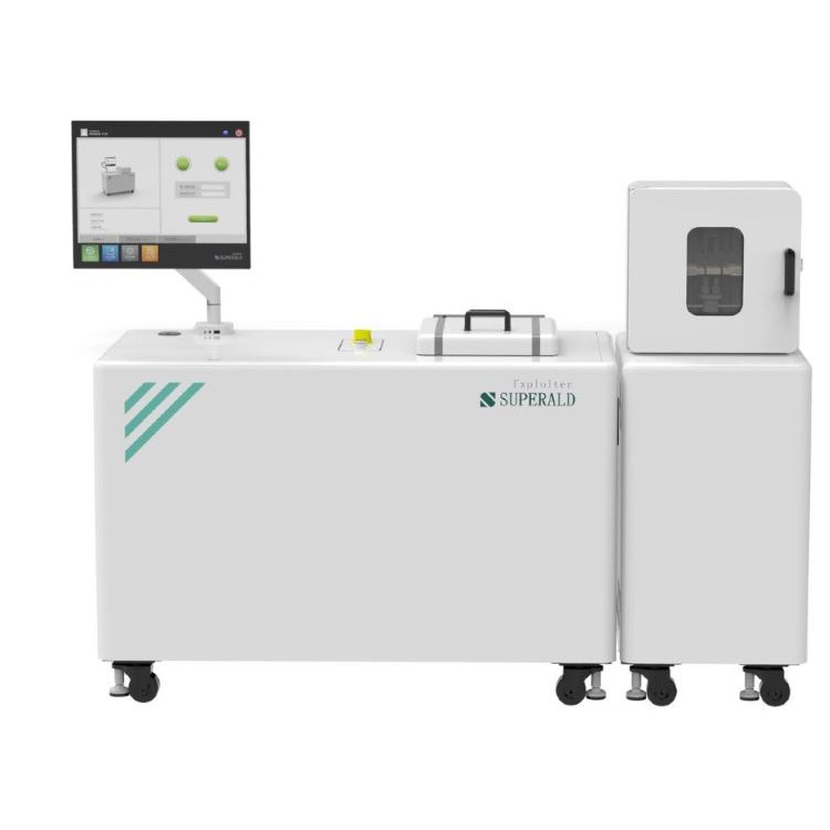
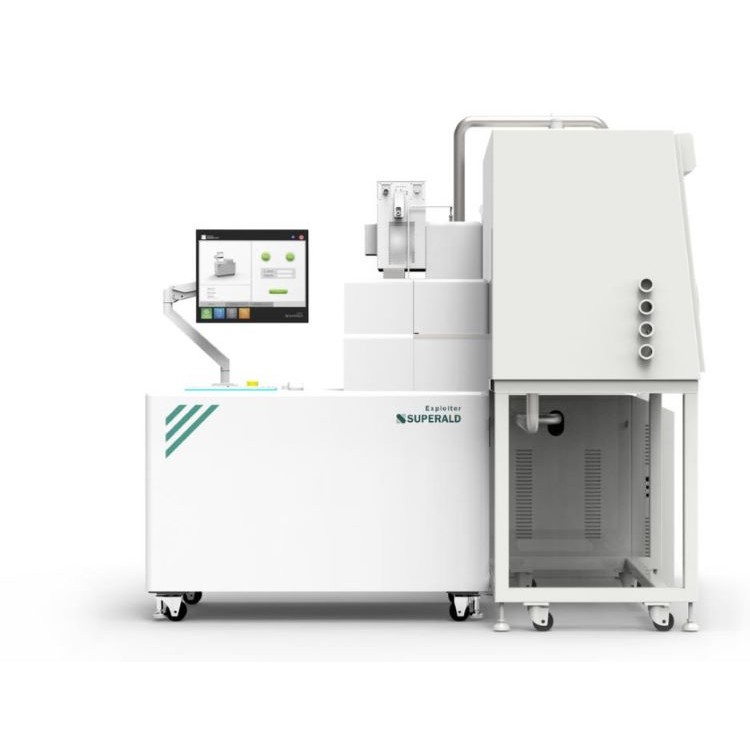


Product Information
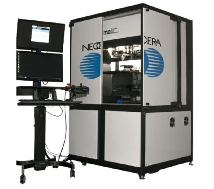
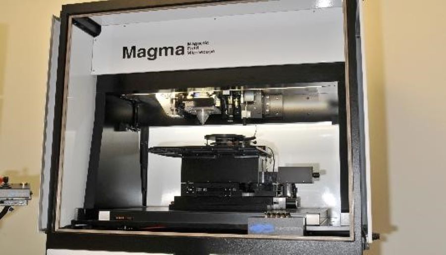
The Magma Magnetic Field Imaging Microscope System (abbreviated as Magma) is a new semiconductor failure analysis tool developed by Neocera Magma Company. It features a unique set of sensors and technology capable of detecting and locating all static defects.
Magma boasts excellent reliability and is suitable for detecting open circuits, short circuits, leakage, and high-resistance open circuits. Additionally, magnetic field imaging can be used to generate depth information for 3D fault analysis, and it can even be applied to multi-layer devices.
In the semiconductor failure analysis field, Magma can locate all static defects in microelectronic systems (short circuits, leaks, and open circuits). It accommodates die-level interconnects on 300mm wafers, packaged PCBs, and all types of packaged devices, including various multi-chip module devices with heterogeneous integration, stacked devices, 3DICs, and SiPs.
The design of the new platform incorporates end-user input to offer user-friendly settings and operations, along with increased workloads and reduced operational costs.
Basic Configuration: Equipped with a highly sensitive SQUID sensor for low current detection, non-destructive short-circuit, leakage, and high-resistance open circuit. It allows for cost-effective location identification, suitable for detecting short circuits and leakages in packaged devices and PCBs.
EFI Tool: Capable of detecting open circuit faults with high accuracy.
HiRes Tool: Combines two sensors into one tool. During current scanning, the SQUID sensor is used to detect the smallest possible current, while the magneto-resistive sensor provides spatial resolution. Therefore, it offers two-fold advantages: spatial positioning and sensitivity.
Application Fields
Magma SSM is a single-magnet sensor system that generates the current image of the device at the封装 and PC board levels. The instrument utilizes a superconducting quantum interference device (SQUID) to detect currents as low as picoamperes in devices, which are then combined to form an image. This image, along with optical benchmarks and design data, can be used to locate three-dimensional static defects.
This electromagnetic imaging is non-destructive. Since most materials used in typical equipment are permeable to magnetic fields, no form of reprocessing is required on the equipment to start fault location. Additionally, using such a small current can protect the device under test from further damage and may be the choice when attempting to detect circuit faults with very high resistance (100k ω). Typical faults that this instrument can analyze include short circuits, leaks, and open resistances. The system can be used for imaging AC and/or DC magnetic fields (current, as well) depending on the equipment's requirements.
Technical Specifications
| Features | Details |
| Squid Sensor | |
| Short-Circuit Defect Location (SQUID) | 3um |
| Spatial Resolution (SQUID) | 2um |
| Total Scanning Area (SQUID) | Not less than 100mm x 100mm |
| Current Sensitivity (SQUID) | · 500nA @ 333um · 1.5uA @ 1000um |
| Magnetic Susceptibility (SQUID) | 15 pT/√Hz Typical |
| Imaging Depth (SQUID) | 10mm |
| Operating Frequency (SQUID) | DC to 25kHz |
| Other parts | |
| Function generator | ±10V @ 100mA |
| Functional Generator Frequency | DC to 200kHz |
| Lens Resolution | 2um (in NIR or Visible) |
| Power Supply | · 110 - 120V @ 20A · 220 - 240V @ 10A |
| Operating System | Windows 10 64-bit |