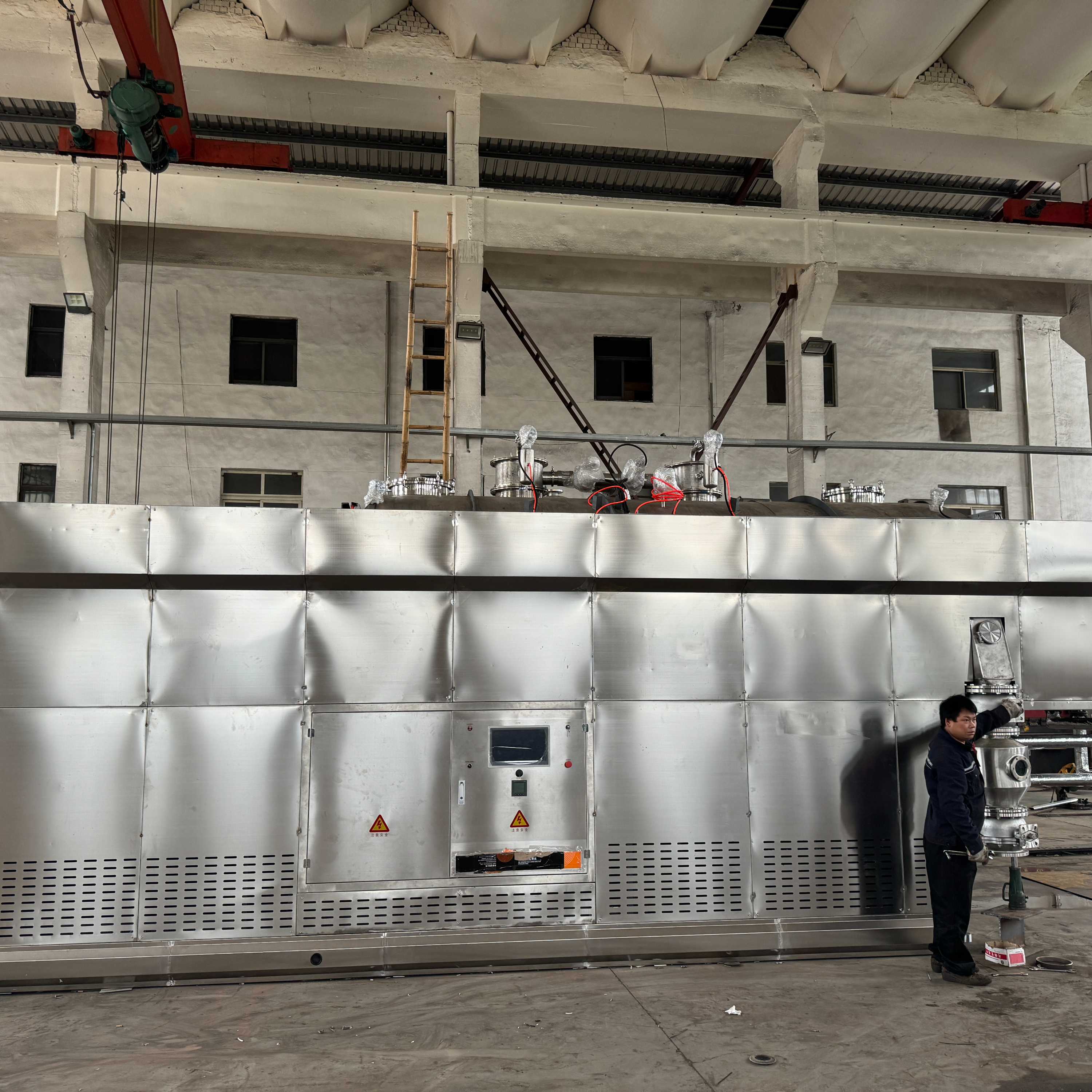

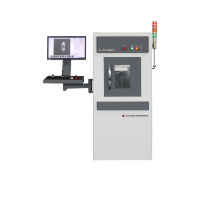


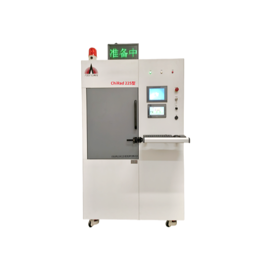
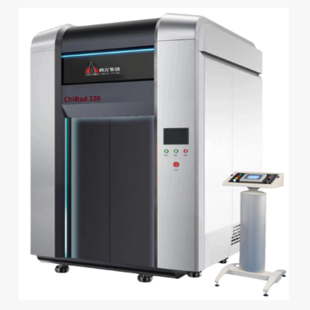
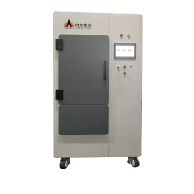


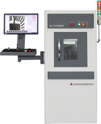
Microfocus X-ray Inspection System
This system is a high-tech product integrating modern computer software technology, precision mechanical manufacturing technology, optical technology, electronic technology, sensor technology, non-destructive testing technology, and image processing technology. It is an effective means for product research, failure analysis, high-reliability screening, quality evaluation, process improvement, and other tasks.
Applicable Range
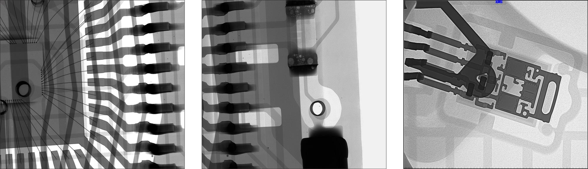
● Suitable for BGA, CSP, and Flip Chip inspection
PCB board welding condition inspection
● Various battery testing
IC Packaging Inspection
● Capacitors, resistors, and other electronic components
● Internal Defects in Metal and Medium Materials
● Internal structure and components of lightweight materials
●Electric heating tubes, pearls, precision components, etc.
Image Processing System Main Functions
●Virtual 3D imaging, real-time zoom in and out
●Gray-scale optimization, real-time pseudo-color, user-friendly design
● Electronic imaging, multi-frame stacking, quick and convenient
Supports positive/negative images, edge enhancement available
● Precise curvature measurement and statistics
Advanced measuring tools
● BGA ball measurement technology
● Angle, radius, weld point area, and bubble area measurements; bubble proportion calculation; weld point coordinate location and statistics
● Dynamic Storage; Multiple Output Methods: Storage, Printing, and DVD Read/Write
Key Parameters
Micro-focus X-ray source
● Tube voltage adjustment range: 20~160kV
● Current Regulation Range: 0.1μA ~ 1000μA
● Focal Sizes: 1μm, 5μm, 30μm
● JIMA resolution: 0.5μm ~ 2μm
● Magnification: 20x to 3000x
●The testing platform can move along the X-Y-Z multi-axis.
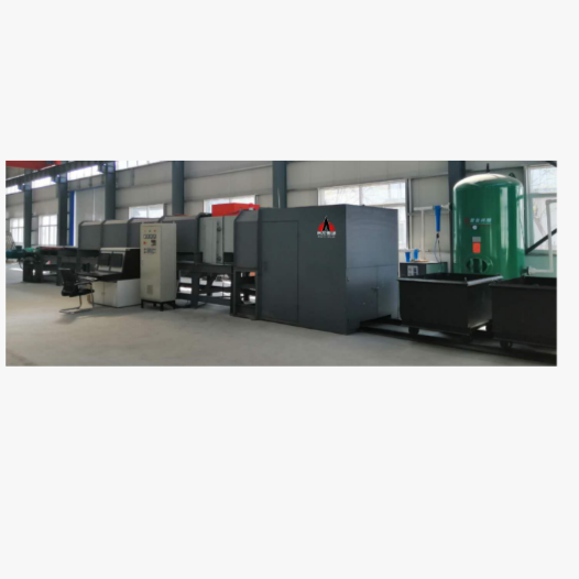
Inspection Case