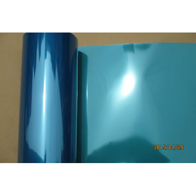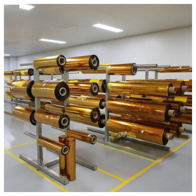


PI (polyimide) film is a high-performance substrate commonly used in flexible electronics and microelectronics packaging fields. By combining the sputtering process, various metal or functional coatings can be formed on the surface of the PI film to achieve a range of functions such as conductivity, shielding, optical properties, or protection. Below isFeaturesWithApplication FieldsA brief introduction to the two aspects of Parylene coating magnetron sputtering.
I. Key Features of PECVD Film Magnetron Sputtering Coating
Low-Temperature Deposition with Excellent Adhesion
Sputter coating is a Physical Vapor Deposition (PVD) technique that, compared to other PVD methods, offers a higher ionization rate and more controllable deposition rate.
Due to the tendency of PI film to warp, deform, or degrade in performance at higher temperatures, controlling the sputtering process parameters (such as target power, substrate temperature, and pressure) reasonably allows for obtaining uniform and well-adhered metal or functional coatings at relatively lower temperatures.
Dense and uniformly high coating layer
Sputtering magnetron can achieve higher uniformity and density films on large-area, flexible substrates like PI films.
For applications requiring fine line widths or high reliability, density and uniformity are crucial, effectively reducing the risk of failure due to porosity or film defects in subsequent processes.
Deposits of various materials
Multiple metal or alloy targets (such as Al, Cu, Ni, Ti, Au, Ag, Cr, etc.) are available, as well as the ability to deposit oxides, nitrides, or alloy materials (such as ITO, TiN, Al-Ni alloy, etc.), to meet various functional requirements.
Achieves monolayer, multilayer, or composite film system designs (such as metal-dielectric layers), providing multifunctional solutions for optical, electrical, corrosion-resistant, and protective applications.
Stress Control and Flexibility Characteristics
The PI substrate is bendable, but the metallic film layer usually has internal stress. If the stress is too high or the film layer is too thick, it may cause cracking and peeling during bending.
Sputter deposition can optimize film stress by adjusting process parameters such as target power, gas flow rate, substrate bias, and temperature, ensuring film performance while attempting to maintain the flexibility of the substrate.
Environmentally friendly and highly automated
The sputtering process utilizes minimal chemical solvents and corrosive substances, ensuring high cleanliness and ease of automation production.
The equipment's process parameters are easy to monitor and replicate, making it suitable for mass and scalable production of flexible electronic devices.
Section 2: Typical Application Fields
Flexible Electronics and Flexible Printed Circuits (FPC)
Depositing metal conductors, pads, or various functional electrodes on the PI film substrate can be applied to flexible circuit boards, flexible displays, flexible sensors, etc.
Transparent electrodes (ITO/metal mesh) for flexible touch screens, Cu/Al thin films for FPC routing, etc.
EMI/EMC Electromagnetic Shielding and Interference Resistance
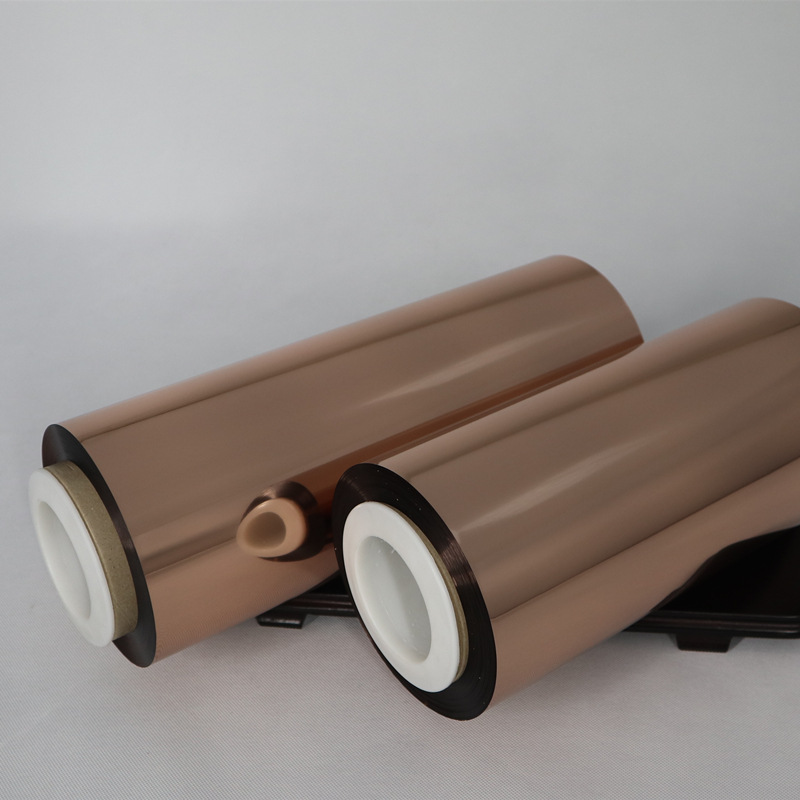
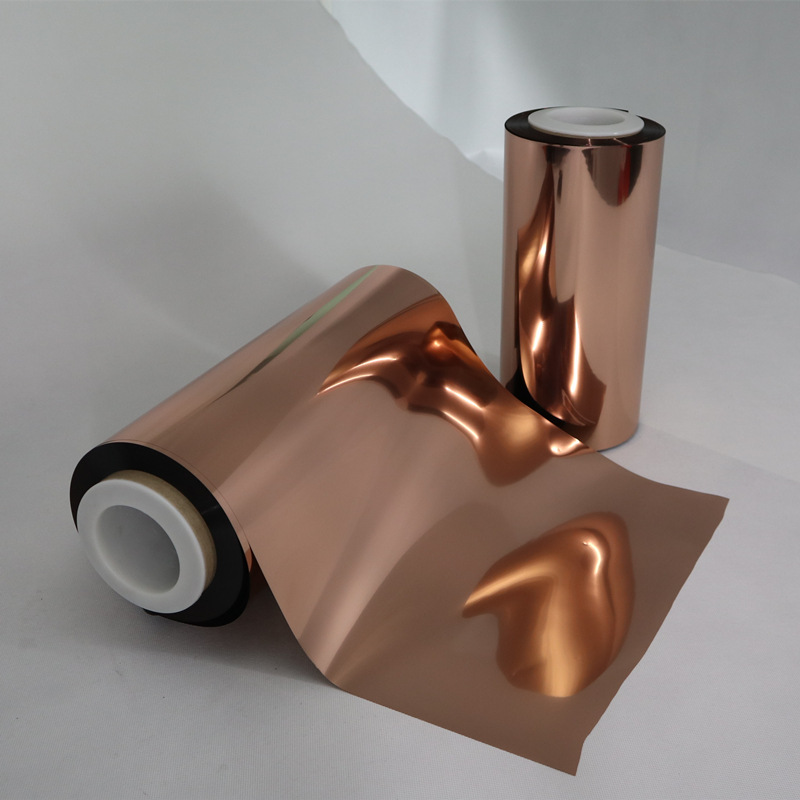
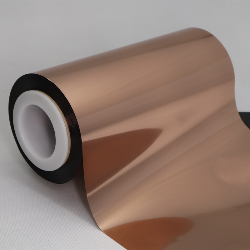
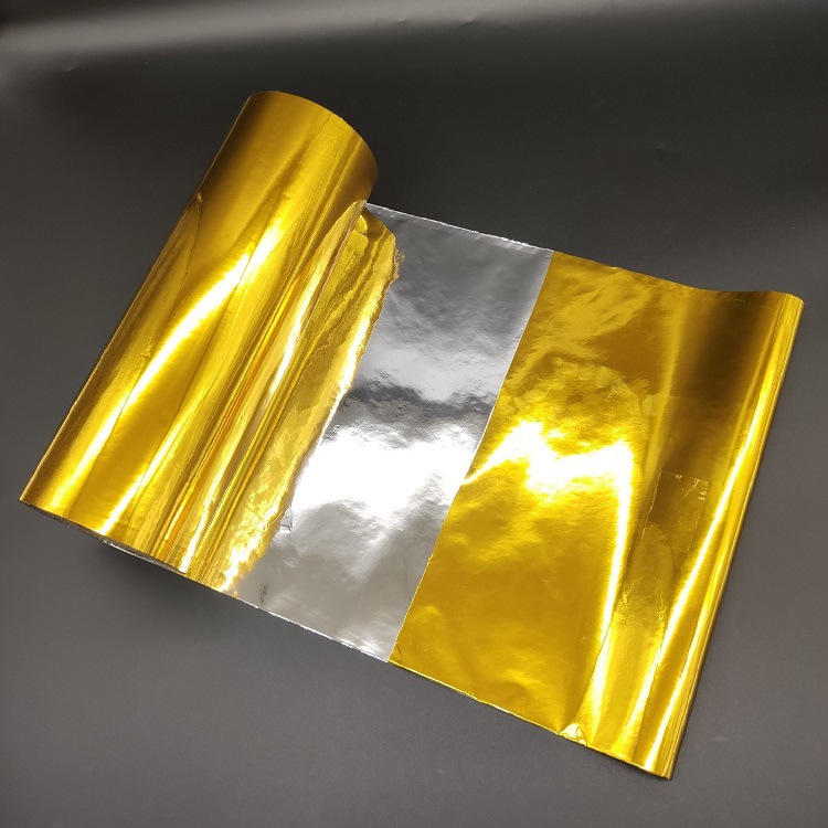
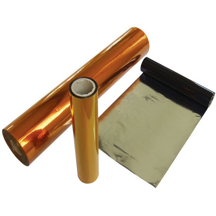
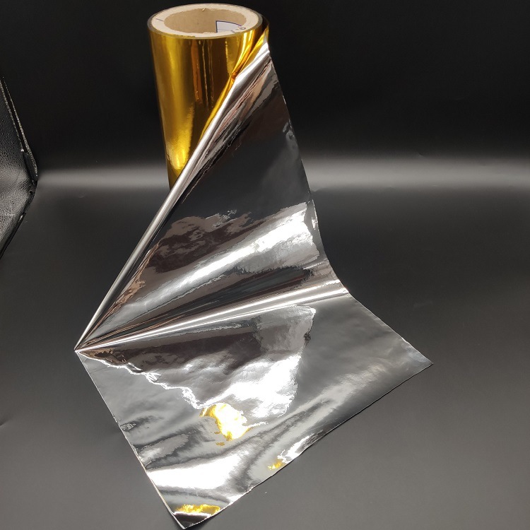
Sputter coating a continuous and highly conductive metal film (such as Cu, Al, Ni, etc.) onto the PI film surface, which can serve as an EMI shielding film.
This metal foil boasts excellent electromagnetic shielding performance, with the base material offering good flexibility, making it suitable for portable devices and wearable tech that are sensitive to weight and space.
Heating film and sensor film
Depositing metals with certain resistive properties (such as NiCr alloys), graphene, or other functional materials on the PI film can produce flexible heating films, which are used in temperature control devices, medical rehabilitation, car seat heating, outdoor equipment, and more.
Flexible sensors, such as strain sensors and gas sensors, can also be formed by sputtering a sensitive film layer onto the PI film surface and subsequently patterning the electrode.
Optical Films and Photoelectric Devices
Sputtering magnetron deposition of ITO, silver nanolayers, etc., on PI film surfaces, suitable for flexible transparent electrodes or reflective film masks.
Used in optical devices or display technologies, such as flexible OLEDs, flexible LCD back electrodes, and touch sensing layers.
High-reliability packaging and protective layer
Some components require dense inorganic films (such as SiO_2, SiN_x) to be applied on the PI film surface for moisture barrier, improved weather resistance, and chemical corrosion resistance; sputtering can achieve high-precision deposition of such inorganic barrier layers.
In harsh environments (such as aerospace and protective electronics), a combination of high heat resistance with excellent wear and corrosion resistance is required. The PI+ sputtering layer often delivers outstanding comprehensive performance.
Special Function Applications
Used for flexible ultrasonic transducers, electromagnetic induction coils, flexible antennas, and more.
In the field of micro-nano processing, micro-structured layers on PI can be fabricated via magnetron sputtering, followed by photolithography or etching processes to achieve high-precision microelectronic component manufacturing.
Section 3: Summary
PI film magnetron sputtering deposition can construct various functional film layers on high-performance flexible substrates, combining advantages such as high-temperature resistance, bendability, and chemical corrosion resistance.Flexible Electronics, EMI Shielding, Optoelectronic Devices, Heating Elements, Sensors, etc.Offered a reliable preparation technology route.
FeaturesLow-temperature deposition, dense film, high adhesion, capable of depositing various functional materials, easy to scale up and automate.
ApplicationWidely usedFlexible Printed Circuits (FPC), EMI Shielding, Optical/Optoelectronic Devices, Flexible Sensors, and Heating Elements, etc., in high-end fields。
As flexible electronics and wearable devices continue to advance, the combination of PI film substrates with magnetron sputtering to produce various functional films will play an increasingly significant role in industries such as electronics, optics, medicine, automotive, and aerospace.