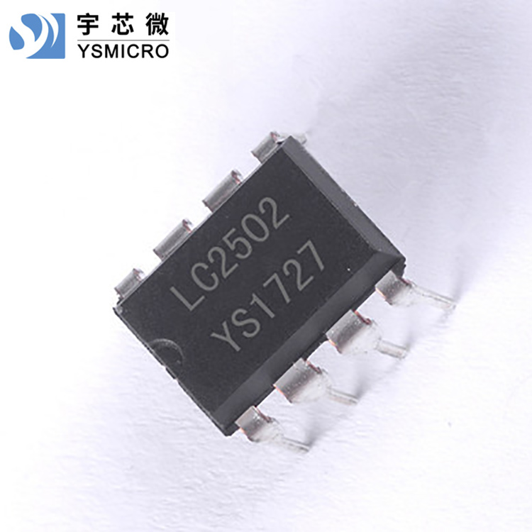


DARLINGTON Driver Circuit LC2502 Overview:
LC2502 is a two-channel Darlington driver circuit with an integrated three-terminal voltage regulator.
The IC integrates a 78L05 three-terminal voltage regulator, providing a stable 5V output power supply. The internally integrated Darlington driver circuit is optimized for switching inductive loads (relays), with an integrated flyback diode capable of absorbing voltage spikes generated during relay de-energization. A single Darlington driver circuit can output 250mA of current, and paralleling Darlington transistors achieves higher output current capability. This circuit is widely applicable to relay driver lighting, display driver (LED), linear drivers, and logic buffers.
Darlington driver circuit LC2502 application:
Relay Driver
LED Driver
Display Driver
Darlington Drive Circuit LC2502's Limiting Parameters:
(Unless otherwise specified, T)A=25℃)
| Parameters | Symbol | Numeric | Unit |
| Drive output end CE voltage | VCE | 30 | V |
| Diode clamp reverse voltage rating | Vd | 30 | |
| Input Voltage | VI | 30 | |
| Collector Current (Continuous Current) | IC | 300 | mA |
| Base Current (Continuous Current) | IB | 20 | |
| Final Temperature | Tj | 150 | ℃ |
| Work Environment Temperature | Topt | -20~+85 | |
| Storage Temperature | Tstg | -55~+150 |
Darrington drive circuit LC2502 electrical characteristics:
(Unless special requirements are specified, T)A=25℃)
| Parameters | Minimum Value | Typical Value | Maximum value | Unit |
| Input Voltage VI | 7 | 25 | V | |
| Output Voltage VOUT | 4.8 | 5 | 5.2 | |
| Load Adjustment Rate (R)LOAD | 0.1 | 2 | % | |
| Voltage Regulation Rate PLINE | 0.5 | 2.5 | ||
| Power Ripple Suppression Ratio R.R | 50 | 55 | dB | |
| Input-Output Pressure DifferenceD | 1.7 | 2 | V | |
| DC CurrentQ | 6 | mA | ||
| CE Saturated Voltage DropC(sat) | 0.8 | 1.1 | V | |
| Output Tube Collector Leakage Current IOLEAK | 1 | 10 | uA | |
| Diode Forward Voltage Drop at Clamp Position | 1.5 | V | ||
| Diode Clamp Current IILEAK | 10 | uA | ||
Input Current II VI=5V | 1 | 2 | mA | |
Input Current II VI=12V | 3.5 | 5 | ||
| Low Input Level VIH | 0.7 | V | ||
| Input High-Level VoltageIL | 2 |