


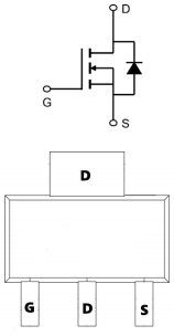
Pinout diagram of domestic MOSFET 4N06:
Domestic MOSFET 4N06's Ultimate Values:
(As otherwise specified, T)C=25℃)
| Symbol | Parameters | Numeric | Unit |
| VDS | Drain-Source Voltage | 60 | V |
| VGS | Gate-Source Voltage | ±20 | |
| ID | Leakage Current - ContinuousContinued TC=25℃ | 4.8 | A |
Leakage Current - ContinuousContinued TC=100℃ | 2 | ||
| IDM | Leakage Current - Pulse | 15 | |
| EAS | Single-pulse avalanche energy | 6.2 | mJ |
| PD | Total Dissipated WorkRate TC=25℃ | 1.5 | W |
| RθJA | Thermal resistance to the environment | 85 | ℃/W |
| RθJC | Thermal resistance to the tube sheet | 48 | |
| TSTG | Storage Temperature | -55~+150 | ℃ |
| TJ | Working Temperature | -55~+150 |
Domestic MOSFET 4N06 electrical characteristics:
(Unless otherwise specified, Tj = 25°C)
| Symbol | Parameters | MIN Value | TYP value | MAX Value | Unit |
| BVDSS | Leakage-Source Emitter Breakdown Voltage | 60 | 65 | V | |
| RDS(ON) | DC On-Resistance VGS=10V,ID=2A | 72 | 95 | mΩ | |
| DC On-Resistance VGS=4.5V,ID=1A | 85 | 100 | |||
| VGS(th) | Gate-Trigger Voltage | 1.2 | 1.5 | 2.5 | V |
| IGSS | Gate leakage current | ±100 | nA | ||
| gfs | Forward Bias Conductance | 13 | S | ||
| Qg | Gate Charge | 5 | 7 | nC | |
| Qgs | Lattice charge density | 1.68 | 2.4 | ||
| Qgd | Grid leakage charge density | 1.9 | 2.7 | ||
| Ciss | Input Capacitor | 511 | 715 | pF | |
| Coss | Output Capacitor | 38 | 53 | ||
| Crss | Reverse Transmission Capacitor | 25 | 35 | ||
| td(on) | Delay Start Time | 1.6 | 3.2 | ns | |
| tr | Initiate ascent time | 7.2 | 13 | ||
| td(off) | Shut-off delay time | 25 | 50 | ||
| tf | Start descent timer | 14.4 | 28.8 |