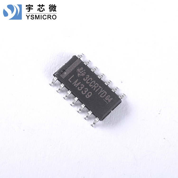


Quad voltage comparatorLM339 Description:
The LM339 is an integrated circuit composed of four independent, high-precision voltage comparators with a low offset voltage of up to 2.0mV. It is specifically designed for wide voltage range applications with a single power supply, and can also be powered by dual supplies. Moreover, the power consumption is very low regardless of the supply voltage. It also features: even with a single power supply, the common-mode input voltage range of the comparator is close to ground level.
Primarily used in limiters, simple analog-to-digital converters, pulse generators, square wave generators, delay generators, wideband voltage-controlled oscillators, MOS clock timers, multi-frequency oscillators, and high-level digital logic gates.
Quad voltage comparatorAdvantages of LM339:
High-precision comparator
Reduce voltage imbalance caused by temperature drift
Single power supply available
Wide input common-mode voltage range
Compatible Logic Circuit
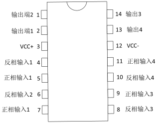
Quad voltage comparatorLM339 Pin Configuration Diagram:
4-channel voltage comparatorLM339's Absolute Maximum Ratings:
Except as otherwise specified, TA=25℃
| Parameters | Symbol | Numeric | Unit |
| Power Voltage (Single Power Supply) | VCC | 36 | V |
| Power Voltage (Dual Power Supply) | ±18 | ||
| Differential input voltage | VIDR | ±36 | |
| Common Mode Input Voltage | VIN | -0.3~+36 | |
| Input Current | IIN | 50 | mA |
| Power Consumption, DIP Package | PD | 1500 | mW |
| Power Consumption SOP Packaging | 830 | ||
| Operating Temperature | TAMB | 0~70 | ℃ |
| Storage Temperature | TSTG | -65~+150 | |
| Bonding Temperature | TJ | +150 |
Four-channel voltage comparatorLM339 Electrical Characteristics:
| Parameters | Test Conditions | Minimum Value | Typical Value | Maximum value | Unit |
| Input Voltage Imbalance VIO | 0℃≤Ta≤70℃ | 2 | 5 | mV | |
| 9 | |||||
| Input失调Current IIO | 0℃≤Ta≤70℃ | 5 | 50 | nA | |
| 150 | |||||
| Input Bias Current IIB | 0℃≤Ta≤70℃ | 25 | 250 | nA | |
| 400 | |||||
| Input Common-Mode Voltage Range VICR | 0℃≤Ta≤70℃ | 0 | VCC-1.5 | V | |
| 0 | VCC-2 | ||||
| Power Current LCC | RL=∞,VCC=15V | 0.8 | 2 | mA | |
| RL=∞,VCC=24V | 1 | 2.5 | |||
| Voltage Gain GV | RL=15kΩ,VCC=15V | 50 | 200 | V/mV | |
| Large Signal Response Time TRES | VIN=TTLLogic Switch, VREF=1.4V,VRL=5V,RL=5.1kΩ | 300 | ns | ||
| Response Time: TRES | VRL=5V,RL=5.1kΩ | 1.3 | us | ||
| Output灌电流 ISINK | VIN(-)=1V,VIN(+)=0,VO≤1.5V | 6 | 16 | mA | |
| Output Saturated Voltage VSAT | VIN(-)=1V,VIN(+)=0,ISINK≤4mA | 130 | 400 | mV | |
| VIN(-)=1V,VIN(+)=0,ISINK≤4mA,0℃≤Ta≤70℃ | 700 | ||||
| Output Leakage Current LOL | VIN(-)=0V,VIN(+)=1V,VO≤5V | 0.1 | nA | ||
| VIN(-)=0V,VIN(+)=1V,VO≤24V,0℃≤Ta≤70℃ | 1000 | ||||
| Input Differential Voltage VID | 36 | V |