


Description: 54123
54123 is a general-purpose residual current protection circuit. It features a differential amplifier, a latch, and a voltage regulator internally, with a high input sensitivity.
Features of 54123:
High input sensitivity (typical value VT=6.1mV)
Good temperature characteristics of input current sensitivity
Peripheral circuit simple
High anti-interference and surge protection capability
Low power consumption (typical PD=5mW), suitable for 110V and 220V power grids
54123's limit value:
Tamb = 25°C, unless otherwise specified.
| Parameters | Symbol | Terms | Numeric | Unit |
| Power Current | ICC | 8 | mA | |
| VRTerminal Current | IVR | VR~IN | 250 | |
| VR~GND | 30 | |||
| IN~VR | -250 | |||
| Terminal Current IN | IIN | IN~VR | 250 | |
| IN~GND | 30 | |||
| VR~IN | -250 | |||
| INLATerminal Current | IINLA | 5 | ||
| Power Consumption | PD | 200 | mW | |
| Work Environment Temperature | Tamb | -20~+80 | ℃ | |
| Storage Temperature | Tstg | -55~+125 |
Note: VR~IN or IN~VRThe current values between them are pulse currents with a pulse width less than 1mS and a duty cycle less than 12%.
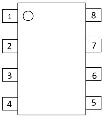
Pinout diagram and pin description for 54123: