


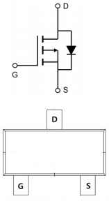
Pinout diagram for low-voltage P-channel MOSFET 2301:
Low-voltage P-channel MOSFET 2301 features:
VDS=-20V
ID=-3.3A
RDS(ON)<80mΩ@VGS=-4.5V
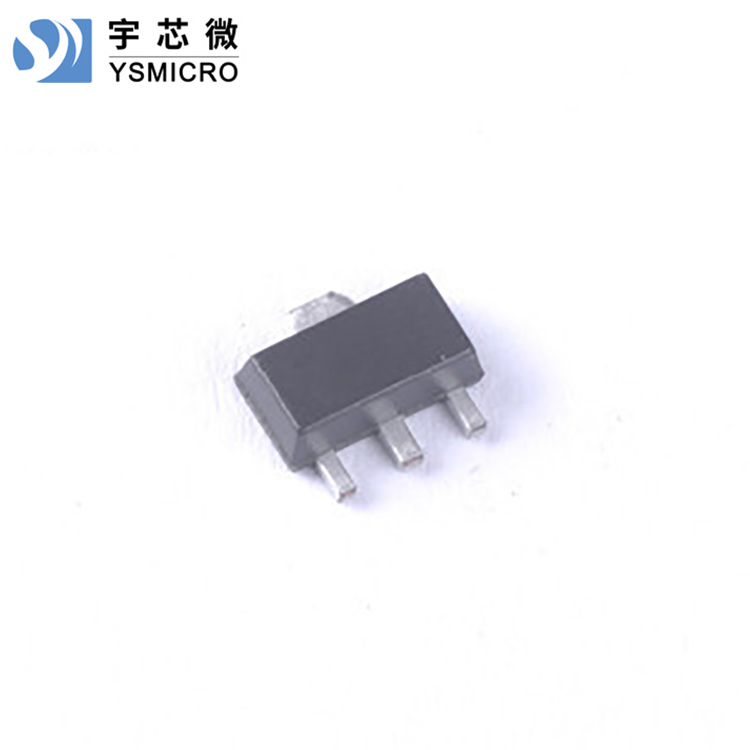
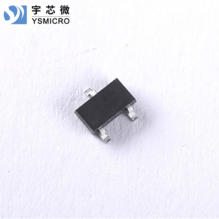
Packaging: SOT-23
Low-voltage P-channel MOSFET 2301 Applications:
Battery Protection
Load Switch
Uninterruptible Power Supply (UPS)
Low-voltage P-channel MOSFET 2301's maximum values:
(As otherwise specified, T)C=25℃)
| Symbol | Parameters | Numeric | Unit |
| VDS | Drain-Source Voltage | -20 | V |
| VGS | Gate-Source Voltage | ±12 | |
| ID | Drain Current - Continuous TA=25℃ | -3.3 | A |
| Leakage Current - Continuous TA=70℃ | -2.6 | ||
| IDM | Leakage Current - Pulse | -13 | |
| PD | Total Dissipation Power TA = 25°C | 1.4 | W |
| RθJA | Thermal resistance to the environment | 125 | ℃/W |
| TSTG | Storage Temperature | -55~150 | ℃ |
| TJ | Work temperature | -55~150 |
2301 Low-Voltage P-Channel MOSFET electrical characteristics:
(As otherwise specified, T)J=25℃)
| Symbol | Parameters | MIN Value | Typical Value | MAX Value | Unit |
| BVDSS | Leakage-Source Emitter Breakdown Voltage | -20 | -22 | V | |
| RDS(ON) | Static leakage on-state resistance VGS=-4.5V,ID=-3A | 55 | 80 | mΩ | |
DC Leakage On-Resistance VGS=-2.5V,ID=-2A | 75 | 100 | |||
| VGS(th) | Gate-Trigger Voltage | -0.5 | -0.7 | -1.2 | V |
| IDSS | Zero栅压漏极电Flow VDS=-20V,VGS=0V,TJ=25℃ | -1 | uA | ||
Zero-gate-pressure漏极电流 VDS=-20V,VGS=0V,TJ=55℃ | -5 | ||||
| IGSS | Gate leakage current | ±100 | nA | ||
| gfs | Forward Bias Conductance | 12.2 | S | ||
| Qg | Gate Charge | 10.1 | nC | ||
| Qgs | Lattice charge density | 1.21 | |||
| Qgd | Grid leakage charge density | 2.46 | |||
| Ciss | Input Capacitor | 677 | pF | ||
| Coss | Output Capacitor | 82 | |||
| Crss | Reverse Transmission Capacitor | 73 | |||
| td(on) | Delay Start Time | 5.6 | ns | ||
| tr | Initiate ascent time | 32.2 | |||
| td(off) | Shutoff delay time | 45.6 | |||
| tf | Initiate descent timing | 29.2 |