Low-internal-resistance MOSFET 3415 features:
VDS=-20V
ID=-4.2A
RDS(ON)<37mΩ@VGS=-4.5V
Designed for PWM, load switching, and general applications
Low on-state resistance and low gate charge
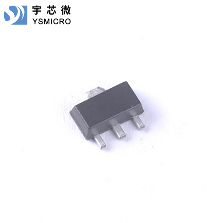
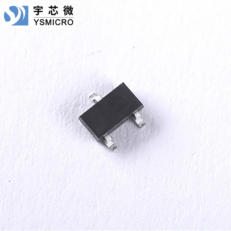
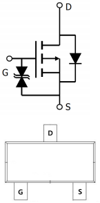
Low Resistance MOSFET 3415 Pinout Diagram:
Low RDS(on) MOSFET 3415's ultimate parameters:
(As otherwise specified, T)A=25℃)
| Symbol | Parameters | Numeric | Unit |
| VDS | Drain-Source Voltage | -20 | V |
| VGS | Gate-Source Voltage | ±8 | |
| ID | Drain Current - ContinuousC=25℃ | -4.2 | A |
| Leakage Current - ContinuousC=70℃ | -2.4 | ||
| IDM | Leakage Current - Pulse | -30 | |
| PD | Total Dissipation Power (T)C=25℃ | 1.4 | W |
| RθJA | Thermal resistance to the environment | 90 | ℃/W |
| TSTG | Storage Temperature | -55~150 | ℃ |
| TJ | Job Completion Temperature | -55~150 |
Low Rds(on) MOSFET 3415 electrical characteristics:
(As stated, unless otherwise specified, T)A=25℃)
| Symbol | Parameters | MIN Value | Typical Value | MAX Value | Unit |
| BVDSS | Leakage-Source Breakdown Voltage | -20 | V | ||
| RDS(ON) | Static leakage on-state resistance VGS=-4.5V,ID=-4A | 37 | 43 | mΩ | |
Static leakage conductance resistance VGS=-2.5V,ID=-4A | 45 | 54 | |||
Static leakage conductive resistance VGS=-1.8V,ID=-2A | 56 | 73 | |||
| VGS(th) | Gate-Trigger Voltage | -0.3 | -1 | V | |
| IDSS | Zero栅压漏极电流 VDS=-16V,VGS=0V | -1 | uA | ||
Zero栅压漏极电流 TJ=125℃ | -50 | ||||
| IGSS | Gate leakageFlow VGS=±8V | ±10 | nA | ||
| Qg | Gate Charge | 10 | nC | ||
| Qgs | Lattice charge density | 0.77 | |||
| Qgd | Lattice Defect Charge Density | 3.5 | |||
| Ciss | Input Capacitor | 939 | pF | ||
| Coss | Output Capacitor | 130 | |||
| Crss | Reverse Transfer Capacitor | 111 | |||
| td(on) | Delay Start Time | 10 | ns | ||
| tr | Turn on the rise time | 8.6 | |||
| td(off) | Shutoff Delay Time | 29 | |||
| tf | Start Descent Time | 13 |
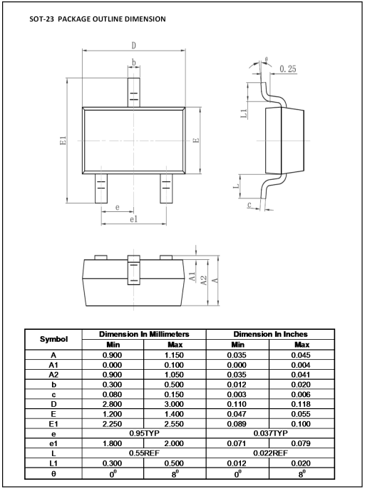
Low-internal-resistance MOSFET 3415 package dimensions diagram: