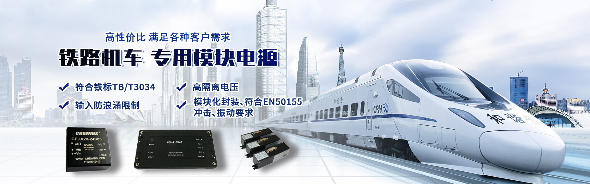
We specialize in the research, manufacturing, and sales of domestic module power supplies, railway power supplies, AC/DC, DC/DC, and DC/AC high-frequency switching power supplies.
15600309099
Modular Power Supply Circuit Design:
In module power supply design, for modules with asymmetric output power, there are two important design methods: one is to use transformer windings and implement a secondary voltage stabilization method by employing coupled inductance and a low-voltage voltage stabilization circuit. The other is to use multiple secondary windings of the transformer to separately output two voltages with relative independence. While the first method can enhance circuit stability and ensure output voltage accuracy, it increases circuit losses. As the input-output voltage difference of the secondary voltage stabilization circuit decreases, the power consumption of the stabilization circuit also decreases.
The project features a significant difference in output power between the two channels, with 55W and 2.5W respectively, and a broad range of power transformation on the main channel. However, if Method Two is employed, since feedback can only control one voltage, the precision of that single output voltage can only be guaranteed. The other voltage must rely on transformer and filter inductor pre-stabilization. Moreover, the large power transformation on the main channel inevitably leads to a significant change in the secondary voltage of the auxiliary transformer, thus making it impossible to ensure the precision of the output voltage. To address this, the design employs two independent output channels for control and feedback, allowing for accurate voltage regulation while also reducing losses associated with secondary stabilization.
Module Power Transformer Design
When designing transformers, the first step is to rationally select the core material. The key factors to consider in the core material are its losses at the operating frequency and the applied magnetic flux density. Once the operating frequency of the power module is determined, you can refer to the manufacturer's manual to identify the specific material model. Then, check the magnetic flux saturation density of the module under harsh operating conditions, and choose a higher magnetic flux density to ensure the transformer never operates at the saturation point. This enhances the reliability of the dc-dc power module. After determining the detailed core model, shape, and size, you can find the magnetic flux saturation density Bs at 125°C. Then, based on derating design, select a magnetic flux density of 0.2Bs. After determining BMAX, you can calculate the primary winding turns of the transformer using the following formula:
In the above equation, Kf represents the wave form coefficient (4 for a square wave), and f is the switching frequency (Hz). Ae is the useful core area (m²), BMAX is the flux density (T), Vi is the input voltage (V), and Np is the primary winding turns. The secondary winding turns of the transformer can be calculated from the primary winding turns:
In the above formula, Np represents the secondary winding turns, and ViIN is the primary low-input voltage. The losses associated with transformers are primarily magnetic hysteresis, eddy current, and resistive losses. Magnetic hysteresis losses are related to the number of turns in the winding and determine the work done by the magnetic force in each operating cycle. These losses can be expressed by the following equation:
In the formula, Kh is the hysteresis loss constant of the material, Vc is the core volume in cm³, fSW is the switching frequency in Hz, and BMAX is the maximum operating flux density in T.
Loss is proportional to the square of the switching frequency and the high value of working magnetic flux density. Therefore, during design, one should not only prioritize cores with high permeability and low high-frequency loss for transformer cores, but also reasonably set BMAX and reduce transformer hysteresis loss by designing the number of turns appropriately.
Design of Module Power Feedback Compensation Circuit
The negative feedback loop is a critical component of switching power supplies, maintaining a constant output voltage is primarily achieved by using an error amplifier to minimize the deviation between the output voltage and the ideal reference voltage, thereby realizing this function. Due to load transitions and input voltage fluctuations in real-world applications, it is required that the error amplifier responds quickly to these changes without causing oscillations that destabilize the entire system.
Module power supply design deviation amplifier compensation circuit should follow the following principles:
Firstly, at all frequencies where the gain is greater than 0dB, the closed-loop phase should not exceed -360°, with a common design choice being less than 300°. The crossover frequency of the closed-loop gain should be as high as possible for website SEO optimization, and the DC gain should be as large as possible, which is beneficial for improving the system's adjustment accuracy and transient response. Furthermore, the slope of the closed-loop gain curve should decrease at -20dB/dec. Due to different control methods used for various power supplies, the corresponding compensation methods also differ. This article adopts a current-type control method and utilizes a pole-zero compensation technique. This compensation method features a pole at DC, which can be improved by increasing the open-loop gain of the error amplifier to enhance the output adjustment performance. Introducing a zero at or below the low pole frequency of the output filter can compensate for the phase lag caused by the filter pole.
Due to the complexity of the dual-output circuit with independent control and feedback, and its high assembly density, interference between leads, between leads and components, and between leads and the housing is inevitably increased. Additionally, as the circuit operates in a switching state, pulsating currents and noise between unit circuits can easily form coupled noise through common impedances such as the power supply's internal resistance and leads. Design-wise, a filter can be added to the circuit to combat coupled noise, and efforts can be made to minimize common impedance in wire layout, properly set ground points, and reduce the power supply's internal resistance to lower noise levels. Furthermore, the flag lighting wires can be scattered away from noise sources and pulsating current-carrying leads to weaken coupled noise.
Secondly, noise generation should be minimized in the design. The short-circuit peak current caused by the reverse recovery time of the switching diode is a significant cause of module noise. During the design phase, a Schottky diode with a faster reverse recovery time can be used, and the appropriate type can be selected based on the detailed output conditions. Proper derating design can also effectively control noise. For noise generated during the operation of high-frequency transformers, decoupling and shielding methods can be adopted in the power module design to reduce interference.
Modular Power Supply Reliability Design
Due to the high quality grade requirements for this product, it must not only pass the QCI inspection from Henan Personnel Examination Website but also the QML inspection. The test conditions are conducted according to the requirements of GJB548A-96 and GJB2438A-2002. The tests undergone by this product are stringent, as it is required to operate reliably over the entire temperature range of -55℃ to +125℃. Therefore, both in circuit design and process structure, reliability design must be considered.
Modular Power Supply Reliability Optimization Design
In terms of design, the circuit structure should be simplified as much as possible, balancing circuit performance with reduced variety and quantity of components, and minimizing the reliability reduction caused by component failures. Furthermore, after the preliminary design is completed, reliability analysis software should be used for analysis and verification to identify areas for improvement and advancement. Finally, parameters should be reasonably designed to ensure the product operates in optimal conditions.
Module Power Supply Derating Design:
Electrical stress of electronic components includes current stress and voltage stress. The derating design of electronic components can effectively improve product reliability. The derating factor is usually between 0.5 to 0.8 times. For example, with an input voltage of 16 to 40V, the rated voltage of the input capacitor used should be 50V, and it should have a voltage withstand capability of 2.5 times. The output voltage is 5V, and the reverse voltage withstand of the rectifying diode used is 45V. For an output voltage of 10V, the reverse voltage withstand of the rectifying diode chosen is 100V, and so on.
Module Power Supply Thermal Design:
Due to the DC-DC module power supply being a power module and requiring long-term reliable operation at 125°C, thermal design is of critical importance. Thermal analysis software and infrared thermal imagers can be utilized for analysis, design, and improvement during the design process. The detailed technical measures are as follows:
1. The input/output filter circuit can utilize high-reliability ceramic capacitors to replace traditional tantalum capacitors, thereby avoiding the failure of tantalum capacitors under high temperatures.
2. Strive to improve product compliance. The use of low-power components and the rational design of transformers can effectively reduce the internal power consumption of the product, while also reducing its temperature rise. During the miniaturization design, the heat sources should be evenly distributed in terms of layout, such as VMOS tubes and rectifier tubes, to avoid concentrating heat in a specific area of the product.
Ensure sufficient contact between the heat source and the substrate, and between the substrate and the housing. Use a current-carrying welding method instead of an adhesive method, if permissible, to reduce thermal resistance and avoid heat accumulation in the product.
Modular Power Supply Technology Design
1. The technology can utilize thick-film multi-layer wiring process, with wiring layers exceeding three. The linewidth and spacing can be 200μm. The resistors in the circuit should commonly be selected as film resistors, and laser trimming technology should be adopted to achieve the resistance values required by the circuit design.
2. Due to the product's high shell temperature of 125°C, controlling moisture content is a challenge. Through the modification of relevant equipment, process research, and repeated experiments on vacuum baking process parameters, appropriate data can be obtained to effectively control the atmosphere during sealing, ensuring that moisture content is less than 5000 pm and oxygen content is less than 2000 pm, thereby ensuring the product's reliability for long-term use.
3. Within the internal structure of module power supplies, there are definite thermal stresses between the substrate and the housing, as well as between the substrate and the components. To meet the high-grade requirements of the product, it is necessary to analyze stress concentration points and mechanical strength. By designing the metalization of the substrate and controlling the thickness of the surface film, the stress conditions between the substrate and the base can be satisfied. Additionally, by selecting appropriate components and using reasonable welding techniques for larger devices, the bonding strength issue between the components and the substrate can also be effectively addressed.
Within the internal structure of modular power supplies, the bulky and heavy components are transformers and inductors due to their fragile magnetic materials and tendency to break. Additionally, there is a significant difference in the coefficient of thermal expansion between these components and the A12O3 substrate. Consequently, in the design, the internal structure can adopt an asymmetric distribution of the substrate to directly affix transformers and inductors to the base. This approach can prevent cracking caused by temperature stress, reduce the area of the substrate to avoid imbalanced gravitational points on the substrate that could lead to cracking during mechanical impact, and also benefit the heat dissipation of the transformers.
4. By selecting appropriate conductive adhesives and epoxy resins, we can research and optimize the matching characteristics between process parameters, operational procedures, and various adhesive and bonding components, thereby achieving high-reliability bonding. For instance, when bonding transformers, using a suitable adhesive not only ensures a certain tensile strength but also exhibits good flexibility. Its temperature characteristics are compatible with the magnetic tank material, ensuring that the tank remains crack-free during temperature cycling.
5. Optimizing welding and bonding techniques. Comparing and analyzing the composition, strength characteristics, and temperature coefficients of solder paste for different models to determine the optimal welding material, ensuring high reliability of the焊接components. Testing the 25μm Au and 200μm Al wire processes can confirm solidification, while also preventing the failure of gold-aluminum wire bonding.
Contact us

Service Hotline
15901068673
Company Telephone
15600309099

Address
25 South Torch Street, Zhoushuizi Economic Development Zone, Baoding City, Hebei Province
b2b.china9.net © Zhongshang 114 Hebei Network Technology Co., Ltd.Address: Room 6009, Oriental New World Center, No.118 East Zhongshan Road, Qiaoxi District, Shijiazhuang City, Hebei ProvincePlatform Service Hotline: 4006299930