


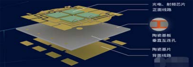
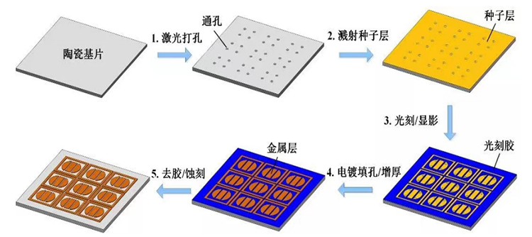
Direct Electroplated Metalized Substrate (DPC)
DPC (Direct Plating Copper) is a foundational electronic material achieved through a magnetic sputtering base coating and electroplating process, enabling metalization of ceramic surfaces and thermal-electric separation.
Advantages
1. Higher thermal conductivity, a more matched coefficient of thermal expansion.
2. Stronger and lower resistance metal film layer.
3. Excellent weldability and high operating temperature.
4. Excellent insulation properties.
5. Conductive layer thickness available for customization within 0.1mm to 1mm.
6. Free of organic components, resistant to cosmic rays, highly reliable in aerospace applications, and boasts a long service life.
7. Capable of high-density assembly line/spacing (L/S) resolution up to 20um, enabling the integration and miniaturization of equipment.
8. Low high-frequency loss, suitable for high-frequency circuits.
9. Electroplated copper sealing, high reliability.
10. 3D Substrate, 3D Wiring.
Application Fields: Automotive Electronics, Industrial Electric Control, Communication Industry, LED Packaging, Gesture Recognition, Facial Recognition, TEC Refrigeration, MEMS Packaging, RF Power Amplifier Packaging, Optical Communication Chip Packaging, Aviation, LED Flashlights, Flash LED, Laser Radar, Industrial Laser Chip Packaging, Infrared, 3D Sensing Cameras, Vehicle LED, UV LED

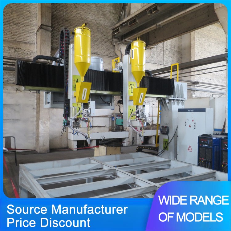
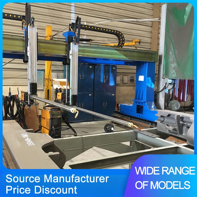
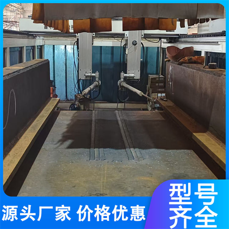
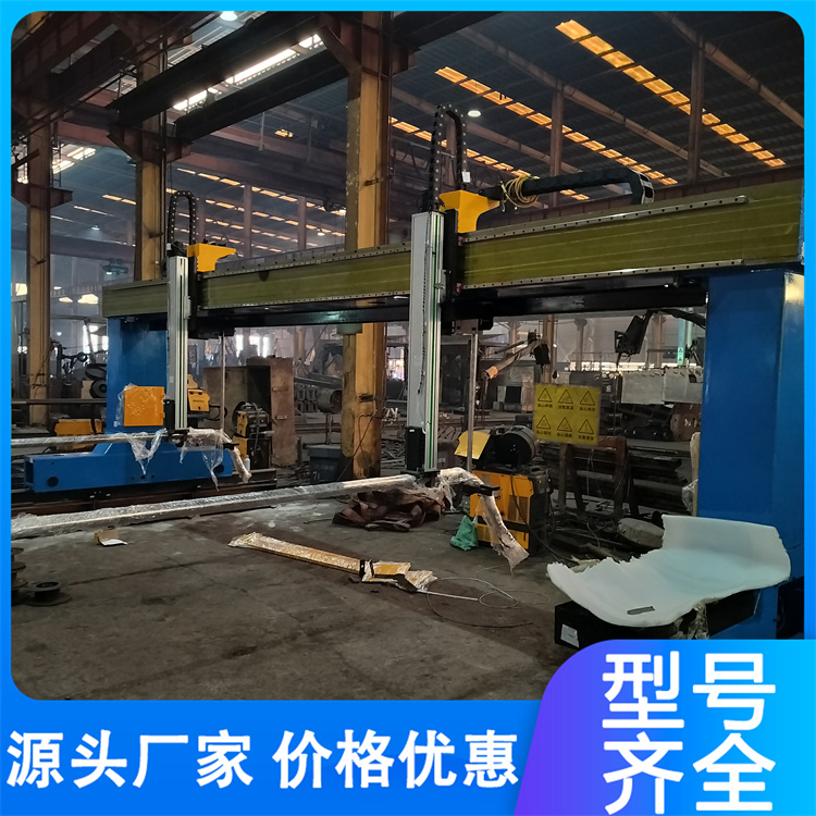
Technical Capabilities
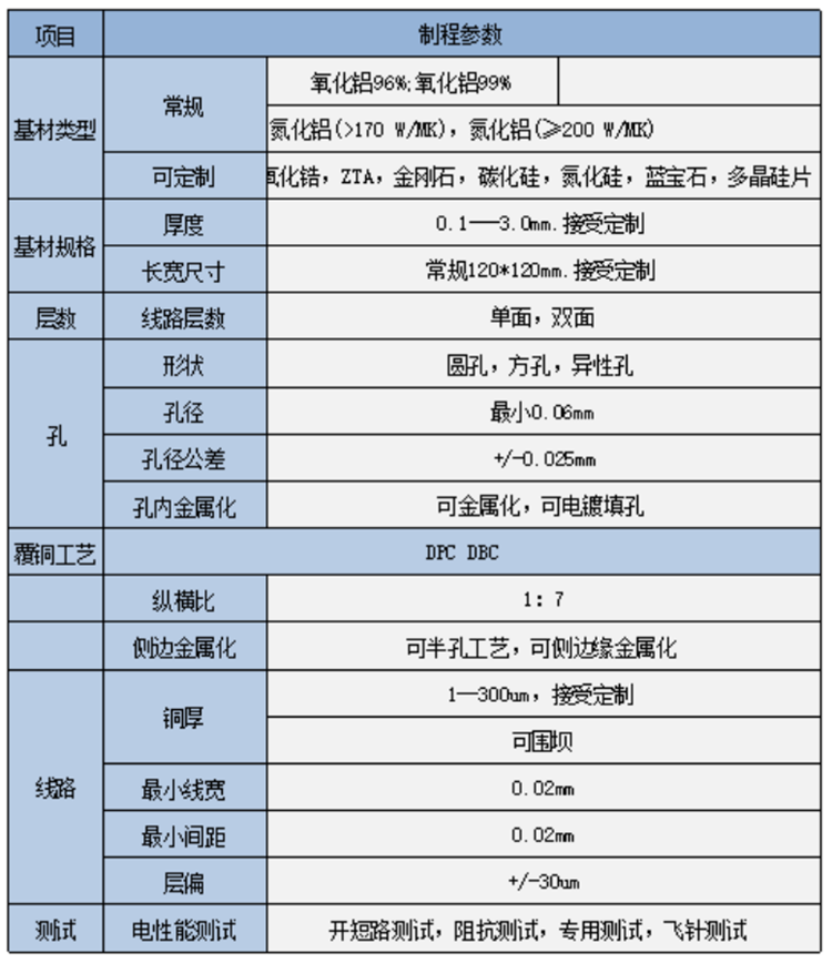
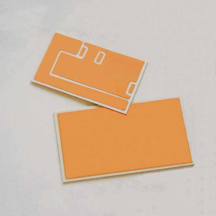
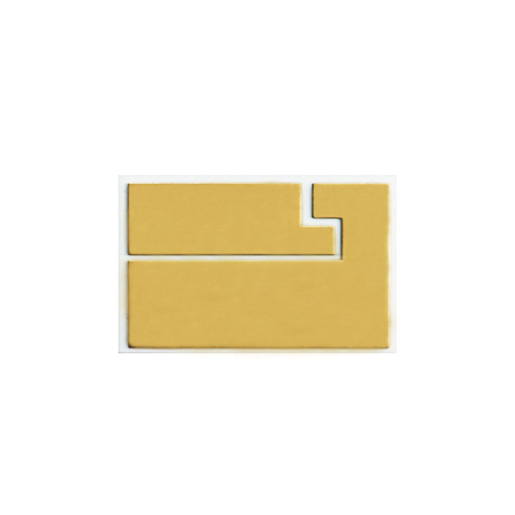
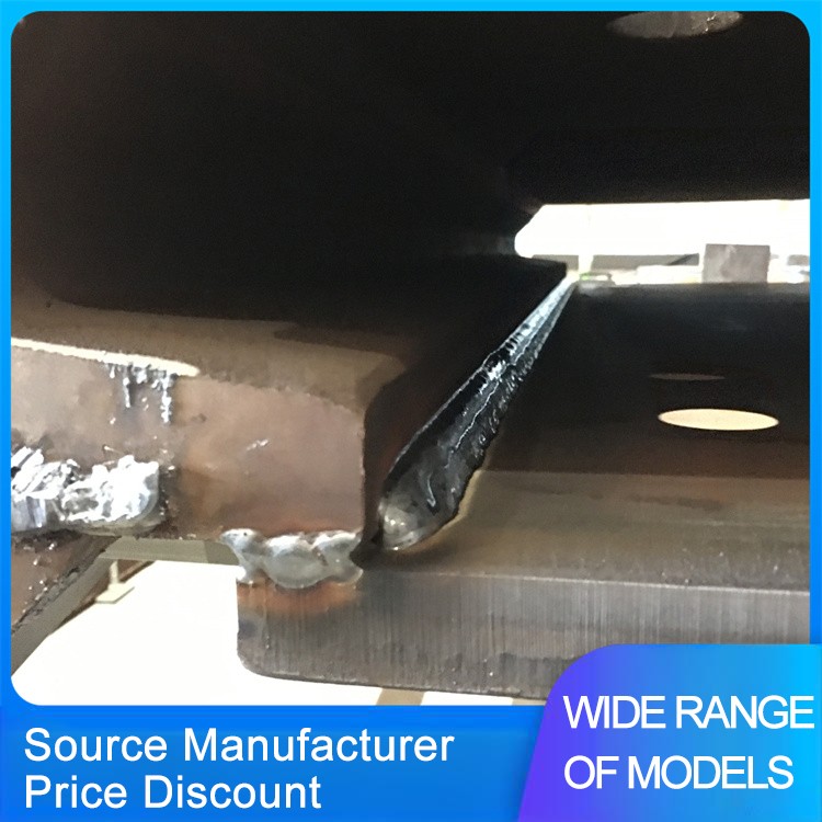
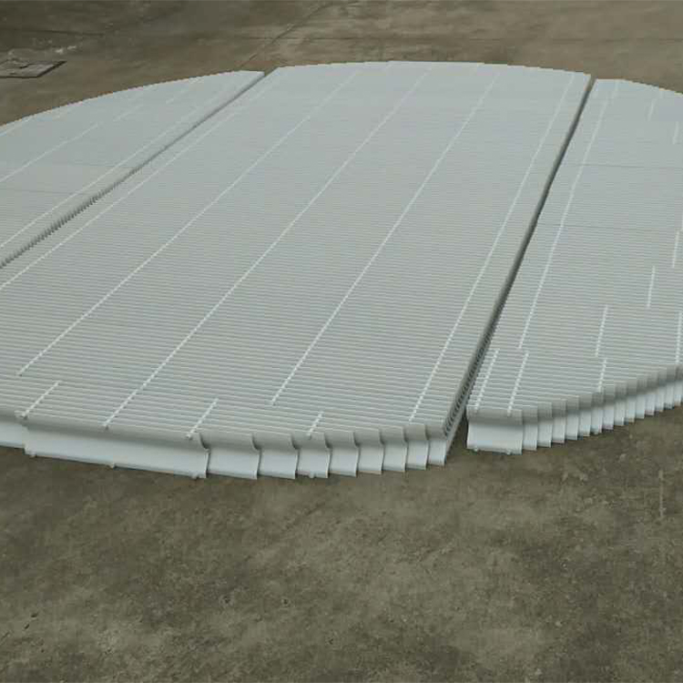
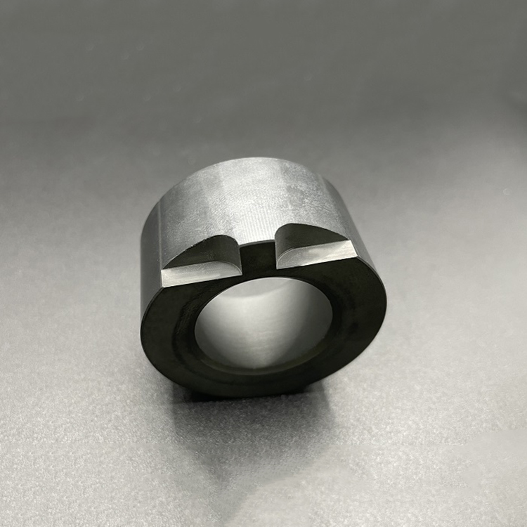
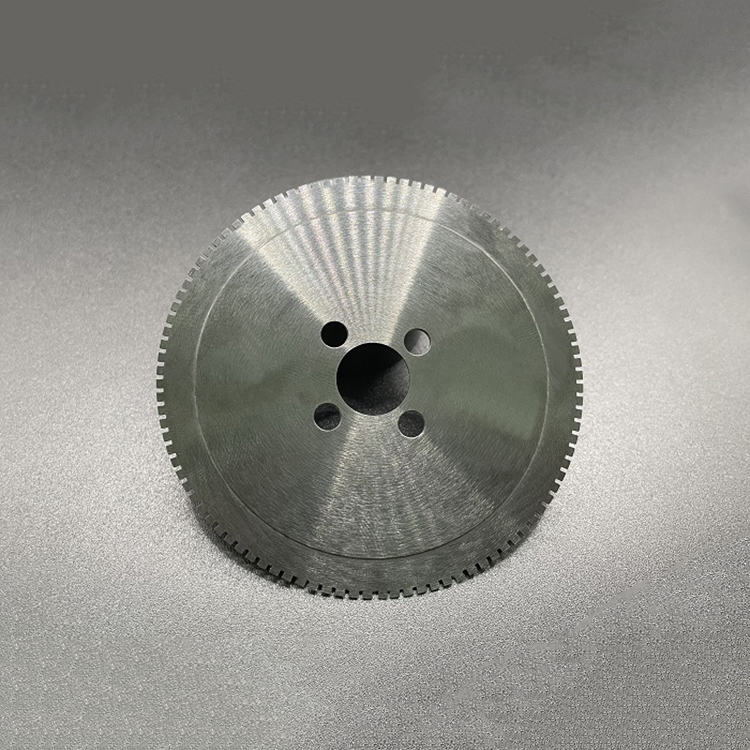
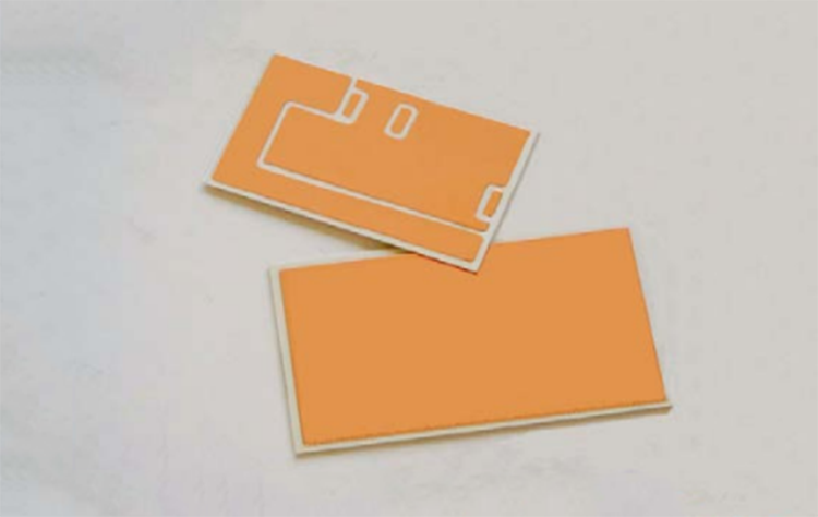
Product Images

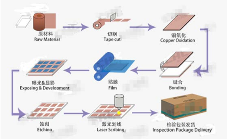
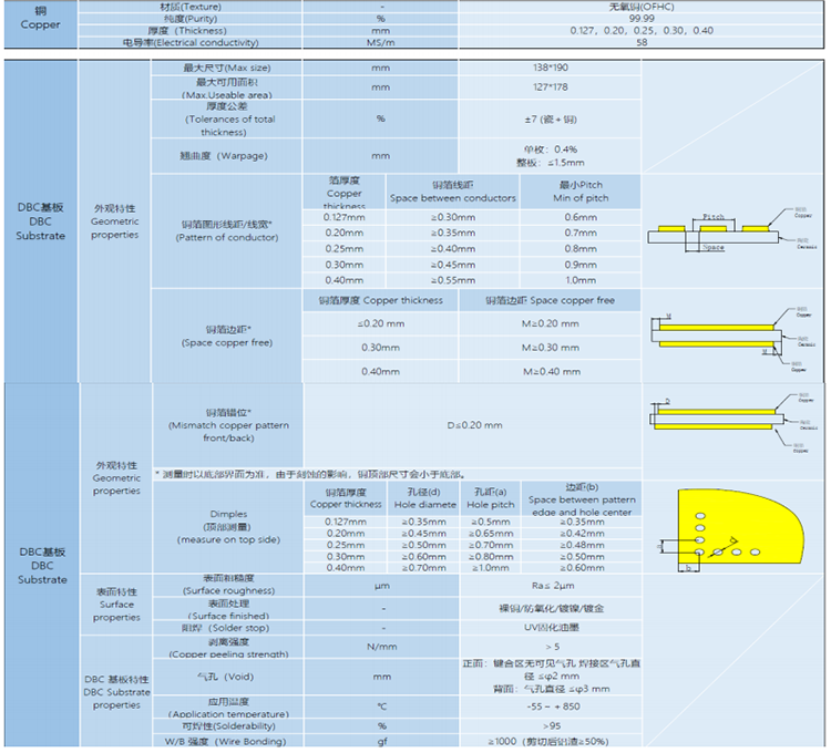
Copper Clad Ceramic Substrate (DBC)
Copper-clad ceramic, also known as copper-clad ceramic substrate, is an electronic base material produced by bonding copper foil directly onto the ceramic surface using DBC (Direct Bond Copper) technology.
Advantages
1. Strong mechanical stress, stable shape.
2. High strength, high thermal conductivity, and high insulation.
3. Strong adhesion, corrosion-resistant.
4. Features excellent thermal cycle performance with up to 50,000 cycles for high reliability.
5. Structures that can be etched into various patterns, like PCB boards (or IMS substrates).
6. Pollution-free and hazard-free.
7. Wide operating temperature range of -55℃ to 850℃; thermal expansion coefficient close to silicon, simplifying the production process of power modules.
Application Fields: The application of DBC ceramic substrates is widely downstream, including semiconductor coolers, electronic heaters, high-power power semiconductor modules, power control circuits, power hybrid circuits, and intelligent power components, as well as high-frequency applications.
DBS ceramic substrates are present in various industrial electronic fields, including switch power supplies, solid-state relays, automotive electronics, solar panel components, telecommunication-specific switches, receiving systems, and lasers.
Technical Capabilities
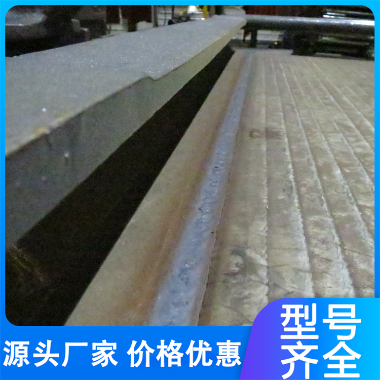
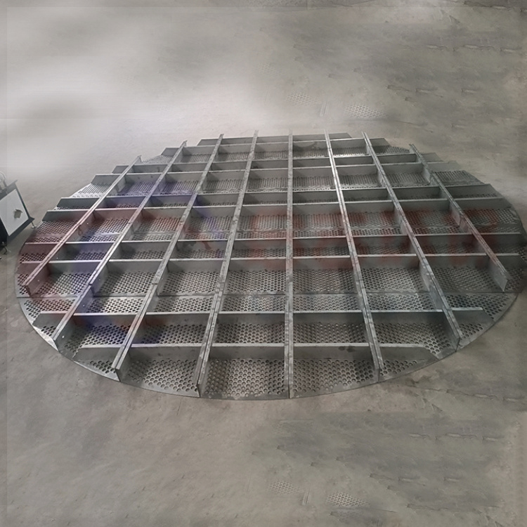
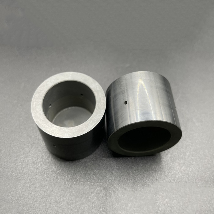
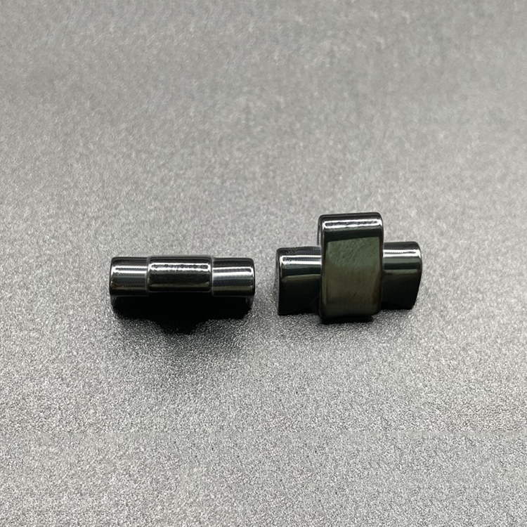
Product Images

Copper-clad Ceramic Substrate (AMB)
AMB technology is an advancement of DBC technology, a method that utilizes the reactive metal elements in the solder (such as Ti/Ag/Zr/Cu) to bond ceramics with metals. The ceramic forms a reactive layer that can be wetted by the liquid solder. Compared to traditional products, AMB ceramic substrates achieve bonding through a chemical reaction between the ceramic and reactive metal solder paste at high temperatures, resulting in higher bonding strength and better reliability. They are suitable for connectors or applications requiring high current carrying capacity and heat dissipation.
Advantages
1. Lower CTE (Coefficient of Thermal Expansion)
2. Possibility of sealed packaging with 0% water absorption
3. Thermal conductivity up to 180 W/m
4. Soldering technology can achieve up to 800 micrometers of copper weight on thin ceramic substrates.
Application Fields: New Energy Vehicles, Power Sports Vehicles, Aerospace, and more.