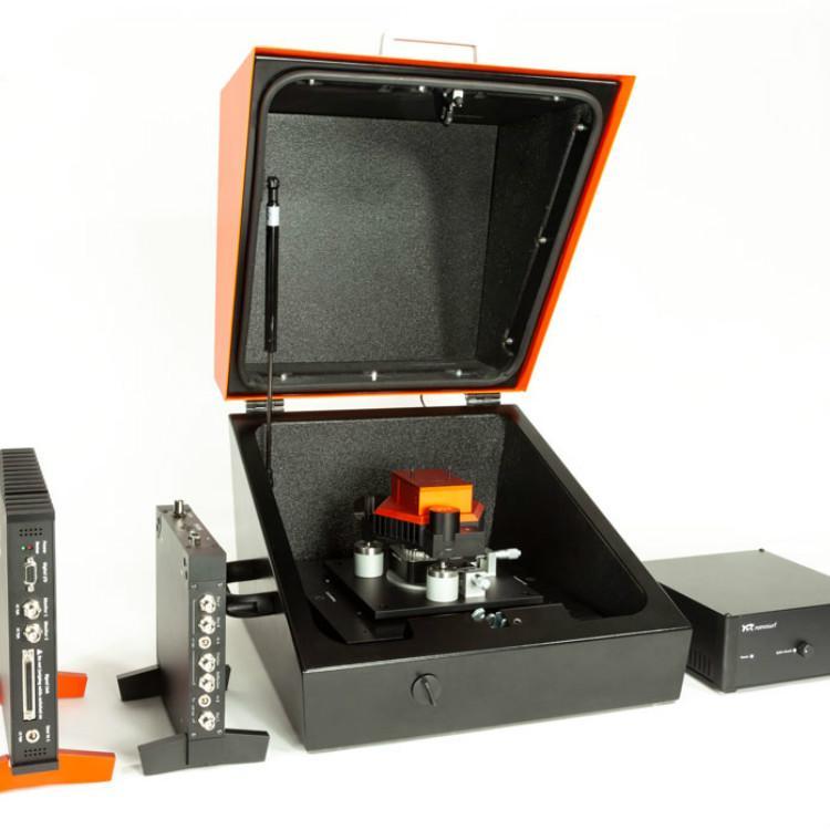
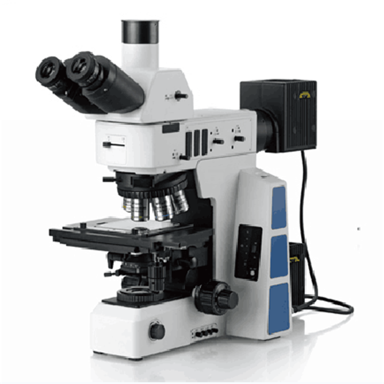
Flex Axiom multifunctional atomic force microscope

Multi functional AFM for material research
● Multi functional atomic force microscope for material research and development
The modular concept can perfectly meet your needs
Suitable for samples of any size
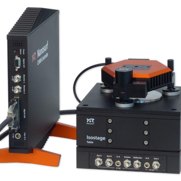
For the success of material research and development, scientists rely on professional tools that can provide the required information at any time, regardless of the task at hand. By advancing key technologies and designs, Nanosurf has made Flex Axiom one of the most versatile and flexible AFMs in history, making it easy to handle various material research applications. Combined with the powerful C3000 controller, complex material characterization becomes achievable.
Hundreds of research users, multiple application examples
Flex Axom is your trusted tool for surface morphology and metrology imaging, whether in atmospheric or liquid environments. Of course, Flex Axom can not only be used for surface morphology measurement, but also for advanced mechanical, electrical, or magnetic characterization. The system has also been successfully used for local sample nanoprocessing.
High accuracy and excellent performance meet your research and development needs
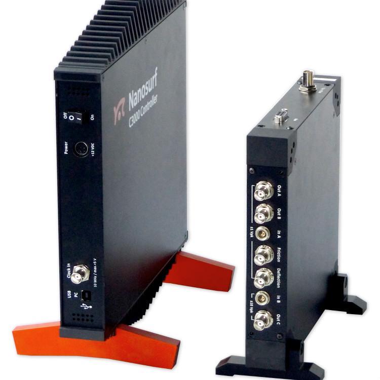
Flex Axiom uses a linear electromagnetic scanning head for XY axis motion. This scanning head achieves an average linear deviation of less than 0.1% across the entire scanning range, making it the top configuration in the AFM market. The Z-axis adopts piezoelectric drive and is equipped with position sensors, which can achieve closed-loop operation. A sensitive cantilever detection system can effectively measure the MHz frequency range. The scanning head is connected to a fully functional 24 bit C3000 controller with digital feedback and 2 dual channel lock-in amplifiers.
Flex Axiom imaging mode
The following describes the modes that the instrument possesses. Some modes may require additional components or software options. For details, please refer to the product manual or contact us directly.
Static force mode
Lateral force mode
Dynamic force mode (tap mode)
Phase imaging mode
Thermal imaging mode
Thermal Scanning Microscopy (SThM)
magnetic properties
Magnetic microscopy
Electrical performance
Conductive Probe AFM (C-AFM)
Piezoelectric force microscopy (PFM)
Electrostatic force microscopy (EFM)
Kelvin Probe Force Microscopy (KPFM)
Scanning Diffusion Resistance Microscopy (SSRM)
mechanical properties
Force spectrum
Force modulation
Stiffness and modulus
adhesion
ductility
Force mapping
Other measurement modes
Etching and Nanofabrication
Electrochemical AFM (EC-AFM)
Application examples
Morphology of SrTiO3 in Dynamic Mode
Strontium titanate (SrTiO3, STO) is an oxide of titanium and strontium, with a perovskite structure. It has interesting and partially unique material properties. It is used as a substrate for the growth of oxide based thin films and high-temperature superconductors. STO forms a layered surface structure. The thickness of each layer is within a range of a few angstroms. Atomic force microscopy is an ideal tool for imaging and measuring these structures.

Display the morphology image of strontium titanate steps, with an image size of 1.1 μ m.

Sectional profile and height distribution
The sample clearly displays the typical layer structure of STO. Here, these layers are not completely smooth, exhibiting a residual roughness (RMS) of approximately 125pm. This is due to the non ideal termination process during the preparation of the STO sample. The middle curve graph shows the contour line of the image shown in the left figure, extending from the upper left corner to the lower right corner of the image area. The contour also clearly displays the layered structure of the sample and reveals a layer height of approximately. 4 Å. Similarly, in the graph on the right, the height distribution histogram on the left clearly shows the peak spacing between different layers of the sample at approximately. 4 Å -.
Morphology and KPFM of CVD grown monolayer molybdenum disulfide film
In this application, Kelvin probe force microscopy (KPFM) using Flex Axiom was used to image monolayer MoS2 grown by chemical vapor deposition (CVD) to investigate changes in contact potential difference on single crystals. Single layer MoS2 is grown on a silicon substrate by chemical vapor deposition (sample provided: University of Illinois Urbana Champlain). The non-uniformity of the surface contact potential signal of the single-layer film can reflect the doping distribution and other surface defects.
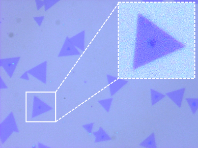
Single layer MoS2 optical micrograph
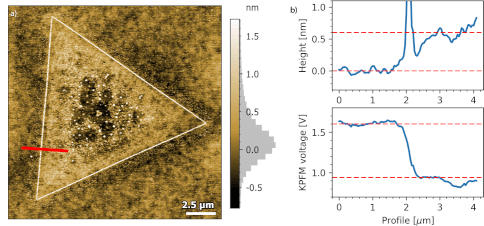
a) The position of the contour of the single-layer MoS2AFM morphology map is marked by the red line
b) Distribution of height (top image) and KPFM voltage (bottom image) on a single-layer film
The step height of single-layer MoS2 measured using Flex Axiom was 0.6 nm. Parallel KPFM measurements showed a contact potential difference of 650 mV between the single-layer film and the SiO2 substrate.

3D AFM morphology overlay with MoS2
In the following experiment, KPFM and morphology data were recorded in one go using the Flex Axiom system. See also related
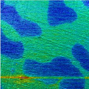
The KPFM diagram of stainless steel is overlaid on the morphology diagram
Scan size: 80 µ m x 80 µ m
Potential range: 200 mV
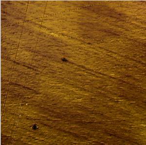
The morphology image itself
Scan size: 80 µ m x 80 µ m
Height range: 50 nm

MFM map of the same region
Scan size: 80 µ m x 80 µ m
Phase range: 10 °