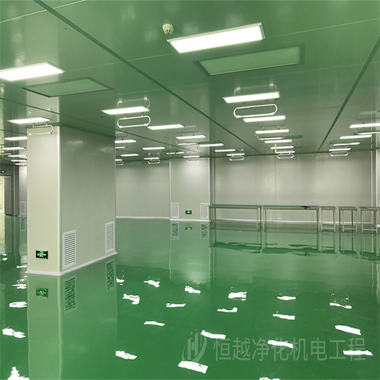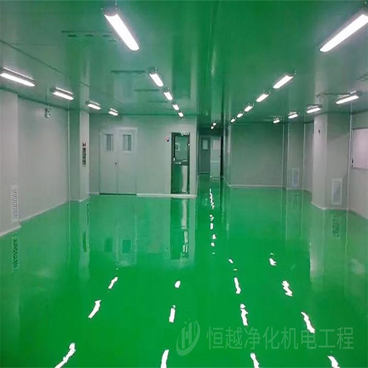
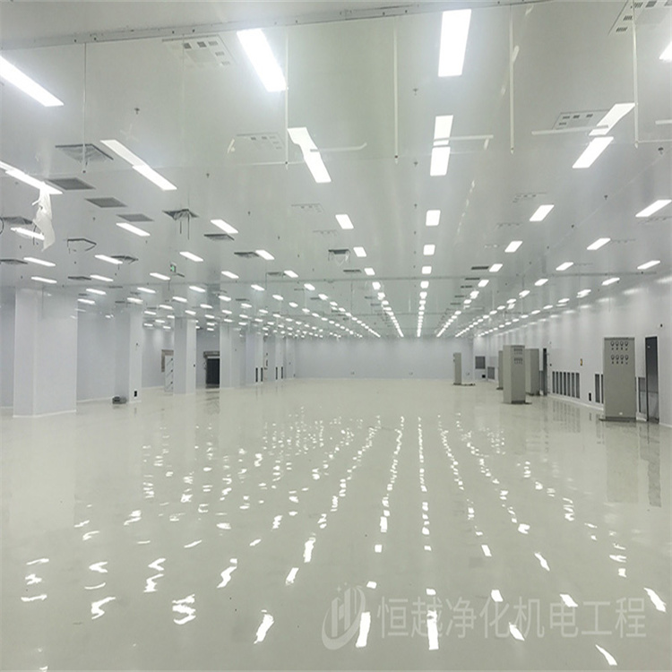


Semiconductor cleanrooms are high-purity environments designed for the production of semiconductor materials and devices, as well as other micro-nano technologies involved in the manufacturing process. These cleanrooms typically feature a very high cleanliness level, with the primary objective of controlling the quantity and size of airborne dust, bacteria, and microorganisms. They also manage factors such as temperature, humidity, and static electricity.

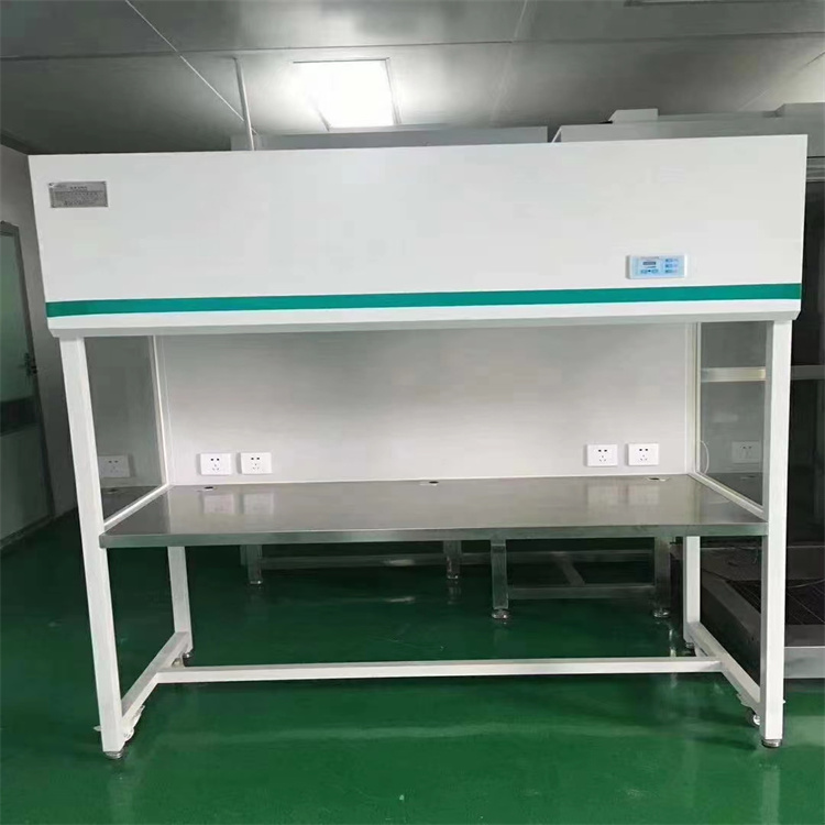
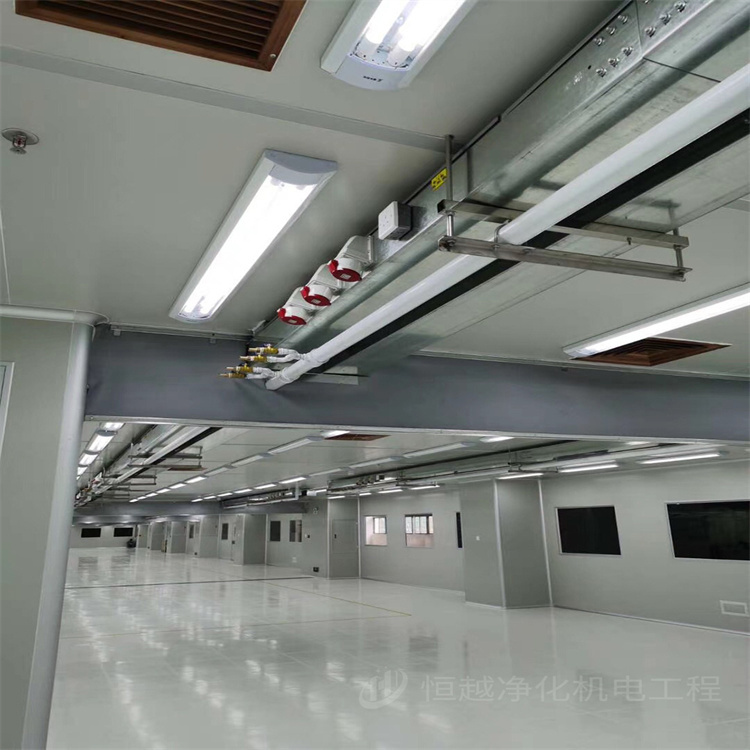
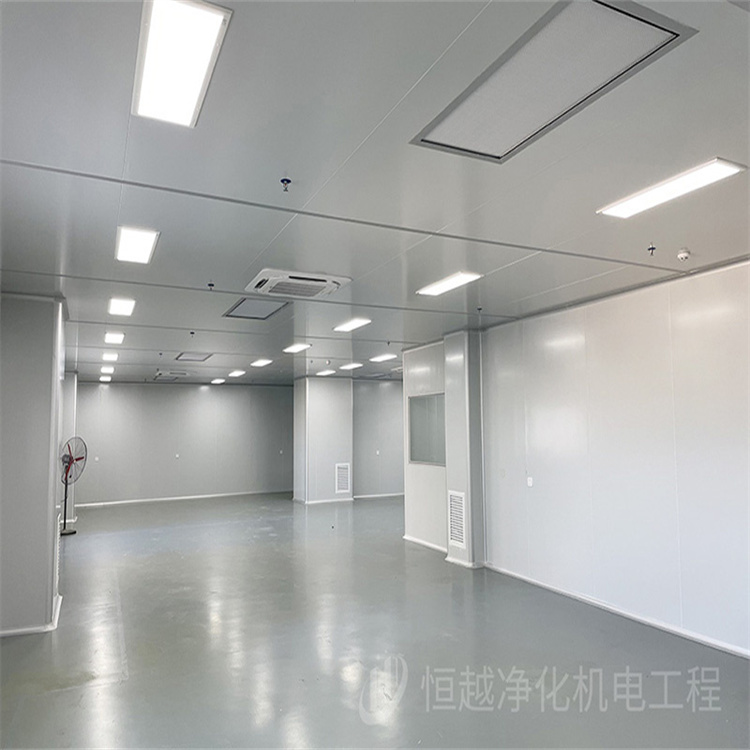
Semiconductor cleanrooms have a structure that differs from typical buildings, typically divided into multiple zones such as entryways, buffer areas, the main cleanroom area, and exits. Depending on their purpose and requirements, additional zones like pre-processing, wet processing, photolithography, cleaning, packaging, and annealing areas may also be included. Moreover, the walls, ceilings, floors, and furniture of semiconductor cleanrooms must be made from high-quality materials and undergo rigorous treatment and protection to ensure the air inside remains free from external environmental contamination.

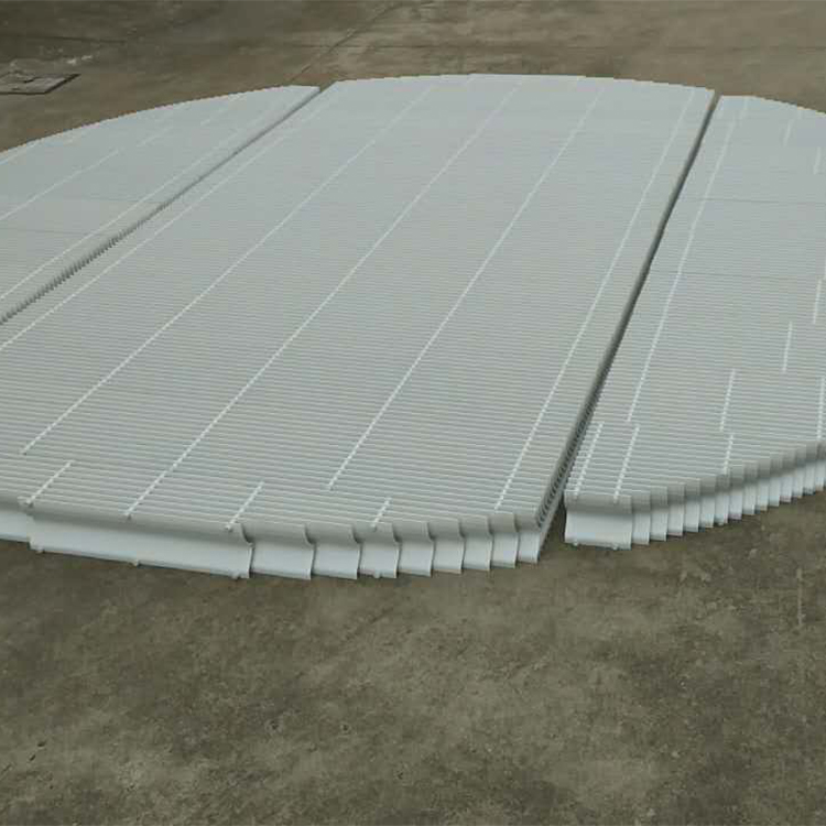
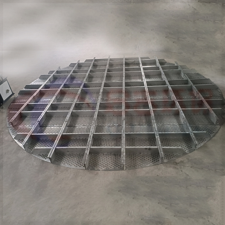
The working principle of semiconductor cleanrooms can be summarized as filtering and purifying the air through a filtration system, which is then circulated to the work area to provide a clean environment. In the cleanroom air system, the filtration system is a crucial component, responsible for filtering out impurities in the air while controlling the direction and speed of air flow. Clean air is supplied to the work area via high-efficiency particulate air (HEPA) filters through ducts to achieve the required cleanliness level for the cleanroom.