| Key Features and Technical Specifications |
| Comprehensive solution for power device characterization, up to 1500 A and 10 kV |
| Medium current measurement and high voltage bias (e.g., 500 mA, 1200 V) |
| μΩ Conductance Resistance Measurement Function |
| At high voltage bias, sub-pA level current measurements can be performed. |
| Automated thermal testing conducted across a temperature range of -50°C to +250°C |
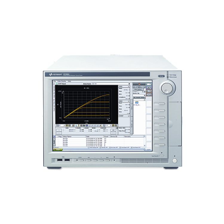
| Comprehensive device measurement capabilities |
| Automatic capacitance measurements (Ciss, Coss, Crss, etc.) can be performed at up to 3000 V DC bias. |
| 10 μs high-power pulse measurement |
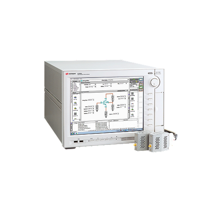
| IGBT/FET gate charge measurement on packaged devices and wafers |
| High-voltage/High-current Fast Switching Option, suitable for GaN Current Collapse Effect Characterization |
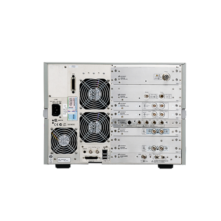
| Up to 5 high-voltage (3 kV) power/metering channels, offering great flexibility |
| Enhanced measurement efficiency |
| Automatically switch between high-voltage and high-current measurements without the need for re-wiring. |
| Automated test circuit formation for measuring the transistor junction capacitances (Ciss, Coss, Crss, Cgs, Cgd, Cds, etc.) on packaged devices and wafer-level components. |
| Standard test fixtures with interlocking mechanism for packaging power device testing |
| Supports high-power wafer testing up to 200 A and 10 kV |
| Oscilloscope view supports verification of applied voltage and current waveforms |
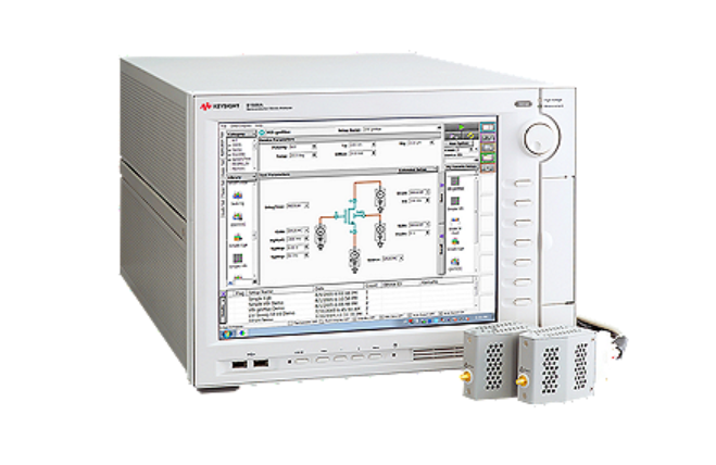
| MS Windows EasyEXPERT software simplifies the data management and analysis process. |
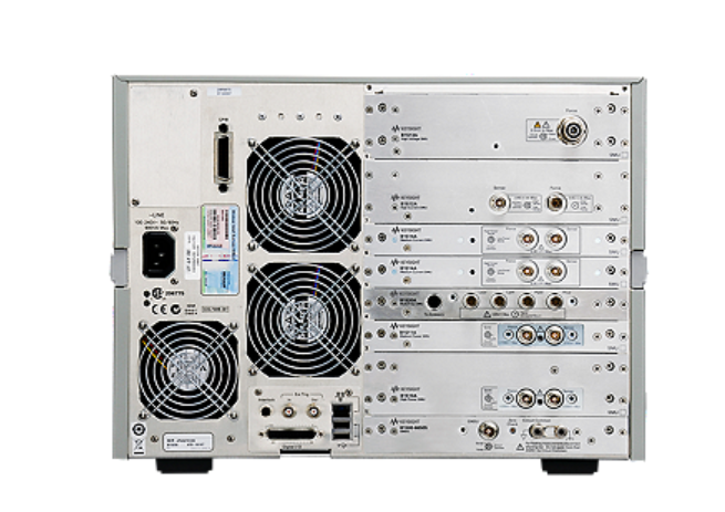
| Upgradable and scalable hardware architecture |
| A wide range of measurement module options |
| Supports high-power devices with up to 6 connection pins |