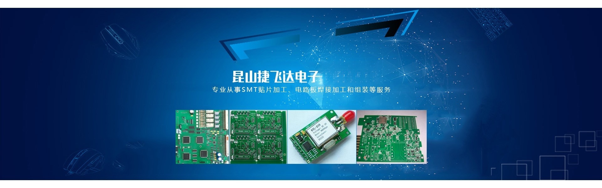
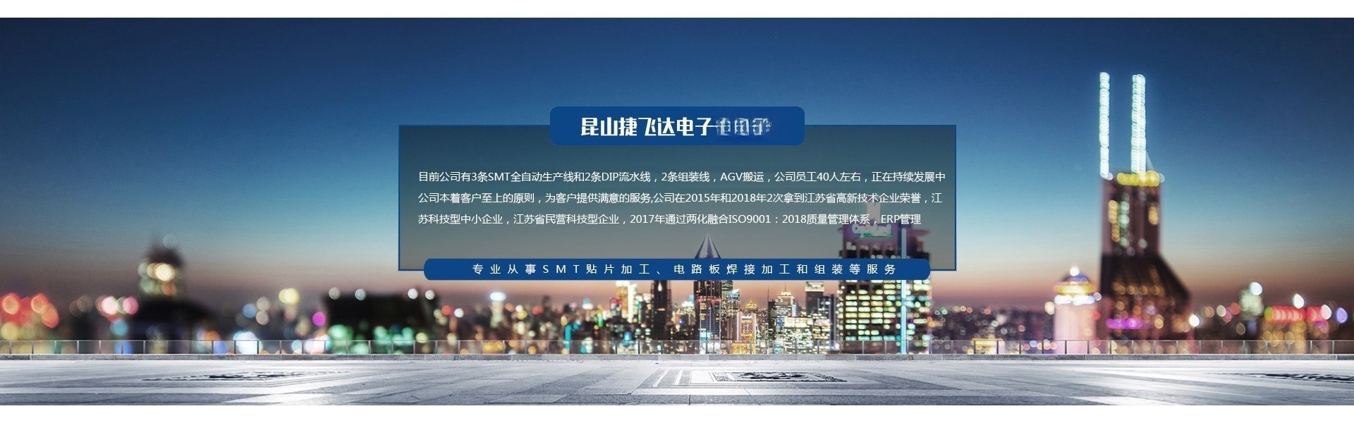
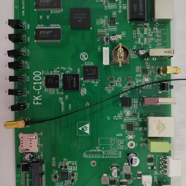
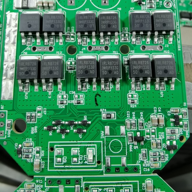
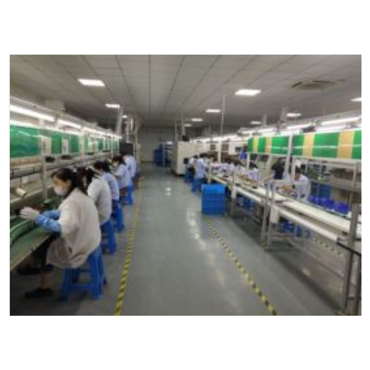
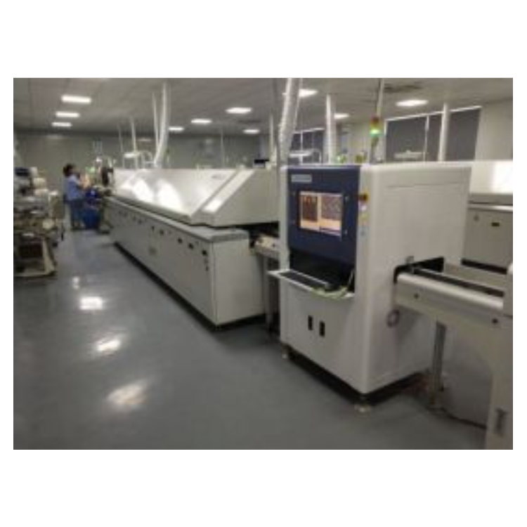
SMT Surface Mount Technology assembly, PCB circuit board welding and assembly
13773198668
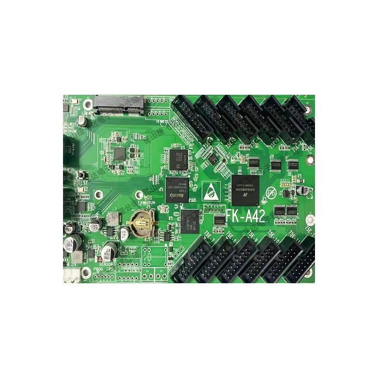
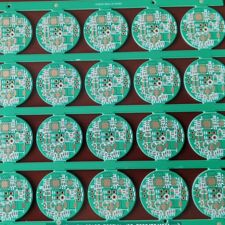
SMT Surface Mount Technology AssemblyThroughout the entire process, there may occasionally be issues with poor production and processing, such as inadequate moisture, bridging, and cracks. These production and processing defects can compromise product quality, reliability, and shelf life. It is crucial for the SMT贴片加工 process to analyze and summarize these defects and prevent similar occurrences in future production. Below is a professional SMT factory...Kunshan JiefiadaBriefly introduce some common defects in surface mount technology (SMT) processing and their solutions.
Insufficient humidity
Poor wettability generally occurs during the entire SMT贴片welding process, where the solder and焊区 on the PCBA board do not transform into a reflection between metal materials after infiltration, leading to common faults such as false welding or insufficient welding.
Solution:
Select appropriate welding processes for PCB assembly welding surfaces and component welding surfaces, implement anti-contamination measures, choose suitable solder materials, and set effective welding temperatures and times.

Two, Qiaoliang
Due to the specific production and processing in the SMT factory, most issues are caused by excessive solder paste or severe edge collapse after the solder paste packaging is printed, as well as dimensional deviations in the base metal plate welding area or misalignment of surface mount components.
Solution:
To avoid poor edge folding during the printing of solder paste packaging.
2. Pay attention to the SMT production processing design specifications when designing the specification for the welding layer of the PCBA board.
3. The surface mount area of electronic components must be within the specified scope.
4. Stringent management is required for the spacing of PCB routing and the precision of solder mask coating.
III. Fracture
SMT Surface Mount Technology AssemblyDuring the initial stage when the board just separates from the welding area, due to the thermal deformation differences between the solder and the closely connected components, under the effects of quenching or rapid heating, the hazards of condensation stress or shrinkage stress may cause micro-cracks in the SMD base. After welding, the PCB must also reduce the impact stress and stress on the SMD during shearing, transportation, and other processes.
Solution:
In the design of surface mount products, it is crucial to consider the differences in thermal expansion and deformation, and properly set the standards for heating and cooling. Use solder materials with excellent plasticity.
Contact us

Service Hotline
13773198668
Company Telephone
13773198668

Address
2 Shanpu West Road, Qianleng Town, Kunshan City
b2b.china9.net © Zhongshang 114 Hebei Network Technology Co., Ltd.Address: Room 6009, Oriental New World Center, No.118 East Zhongshan Road, Qiaoxi District, Shijiazhuang City, Hebei ProvincePlatform Service Hotline: 4006299930