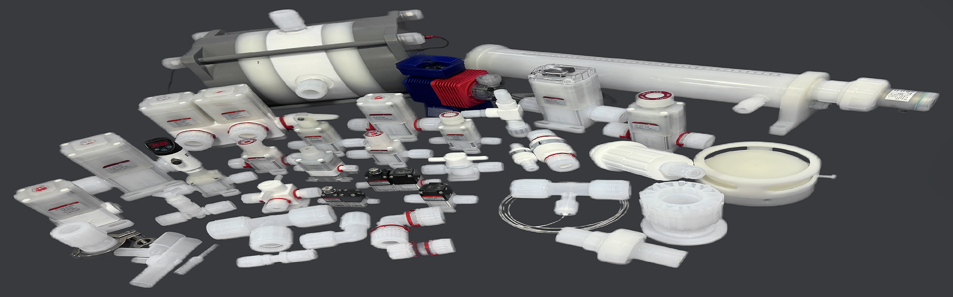
Diaphragm valves, transition connectors, high-purity pipe...

In the grand landscape of the semiconductor industry, materials and equipment serve as a solid foundation and are also a powerful engine driving the continuous innovation of integrated circuit technology. The implementation of one generation of advanced technology relies on a corresponding generation of processes; and the realization of this generation of processes is inseparable from a specific generation of materials and equipment. As a key upstream link in the entire semiconductor industry chain, semiconductor materials play a crucial supporting role in industry development, displaying significant characteristics such as large scale, numerous segmented industries, high technical barriers, substantial R&D investment, and long R&D cycles.

01 The industry boasts a large scale with strong growth momentum.
Semiconductor materials primarily cover wafer manufacturing materials and packaging materials. According to SEMI data, the global semiconductor materials sales reached $63.3 billion in 2021, a 15.9% year-over-year increase from $55.5 billion in 2020. Among them, wafer manufacturing materials sales reached $40.4 billion, while packaging materials sales were $23.9 billion, with year-over-year growth rates of 15.5% and 16.5%, respectively. From a regional perspective, Taiwan, with its robust wafer fabrication and advanced packaging industry foundations, continued to be the largest consumer of semiconductor materials for the twelfth consecutive year with sales of $14.7 billion, growing at a rate of 15.7%. Mainland China, due to its proactive factory construction, achieved semiconductor materials market sales of $11.9 billion, with a remarkable growth rate of 21.9%, surpassing South Korea and securing the second position globally.

02 The industry is highly segmented with a rich variety of product types.
The semiconductor materials industry encompasses a vast array of specialized segments within the semiconductor supply chain. Wafer manufacturing materials include silicon wafers, photomasks, photoresists, ancillary photoresist materials, process chemicals, electronic specialty gases, polishing fluids and pads, target materials, and other materials. Packaging materials cover lead frames, substrate boards, ceramic substrates, bonding wires, encapsulation materials, chip bonding materials, and other packaging materials. Notably, each major category is further subdivided into dozens, if not hundreds, of specific products, with a multitude of sub-industries numbering in the hundreds, highlighting the industry's complexity and diversity.

High technical barriers and significant research and development challenges
Semiconductor materials, particularly wafer manufacturing materials, play a crucial role in the production of integrated circuit chips. Some key materials even directly influence chip performance and the direction of technological development. As a result, downstream customers have stringent requirements for the products. Before being put into use, the products must undergo a long cycle of testing and validation. After launch, they also gradually achieve large-scale application over an extended period. Additionally, before entering the testing and validation phase, the products must go through a lengthy and challenging research and development process, requiring substantial investments in funds and human resources. These factors highlight the industry's characteristics of high technical barriers, significant R&D investments, and long R&D cycles.

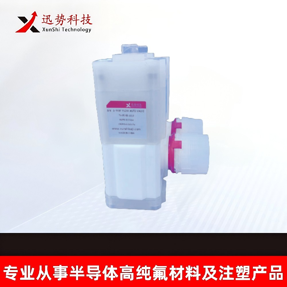
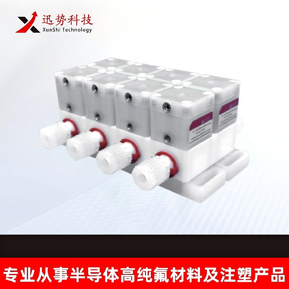
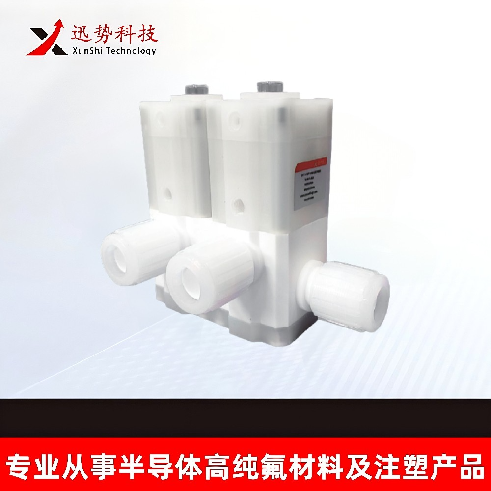
In the challenging yet promising field of semiconductor materials, Unswift Technology is flourishing, striving to become a core force in the industry. We collaborate with our upstream and downstream partners to address material and end-user applications, while also partnering with universities to focus on the systematic development of high-purity fluoro-plastic fluids, such as sensors, pumps, valves, connectors, and pipes. Our mission is to break monopolies, resolve bottlenecks, and work towards the complete domestication of China's semiconductor industry. Unswift aims to systematically address high-purity fluoro-plastic fluid products for semiconductors in the future, to establish a renowned domestic company, and become an international brand, serving more clients.

Data Source: SEMI
About Us
China's Pioneering Company in Fluoroplastic Flow System Solutions
Follow TrendingTech, Unleash the Passion of Trending People!
Media Contact
Xunshi Technology (Suzhou) Co., Ltd.
Phone: 0512-57479960
Email: Sales2@xunshikeji.com
Company News Website:www.xunshikeji.com
Weixun Technology High Purity Fluoroplastic Products


b2b.china9.net © Zhongshang 114 Hebei Network Technology Co., Ltd.Address: Room 6009, Oriental New World Center, No.118 East Zhongshan Road, Qiaoxi District, Shijiazhuang City, Hebei ProvincePlatform Service Hotline: 4006299930