
- AllProduct Category
-
Powder Property Tester
Powder Flowability Tester
Bulk Density Gauge
Loose Density Tester
Pile Density Tester
Apparent Density Meter
Rest Angle Gauge
Rest Angle Gauge
Particle Strength Tester
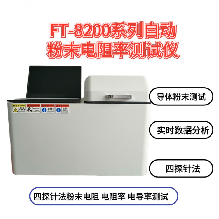
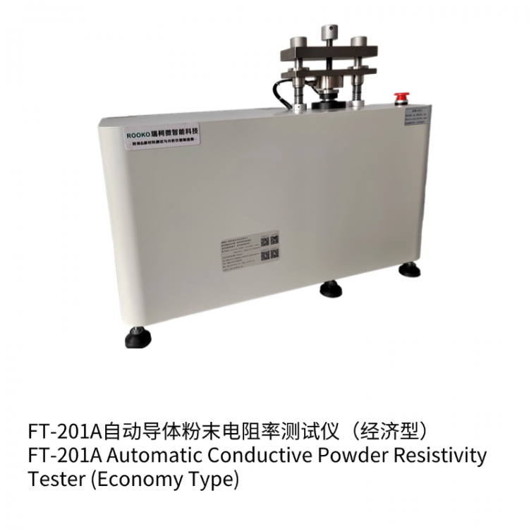
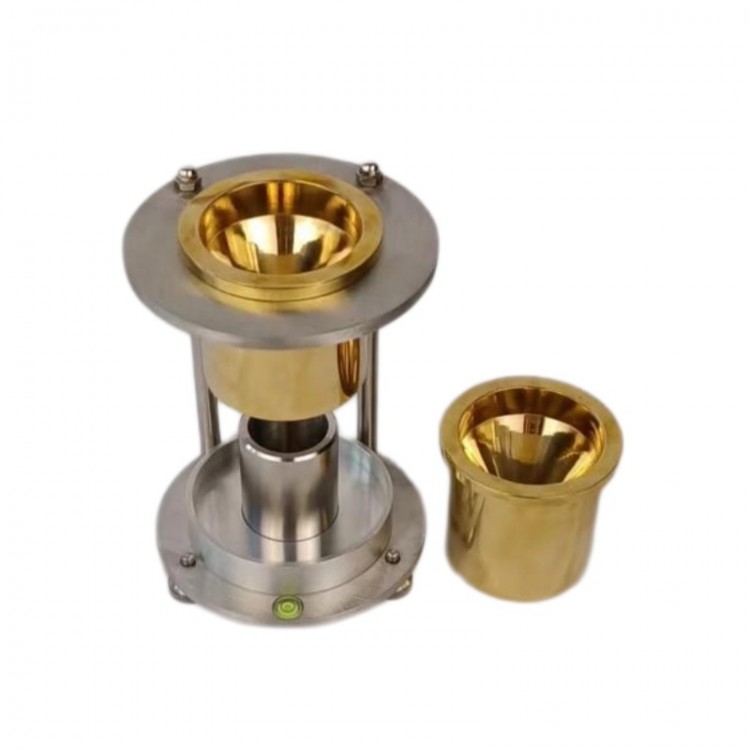
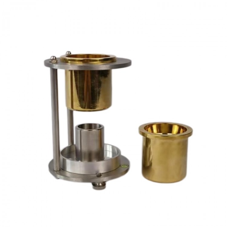
Powder Resistivity Tester
Compaction Density Gauge
Hole Flowmeter
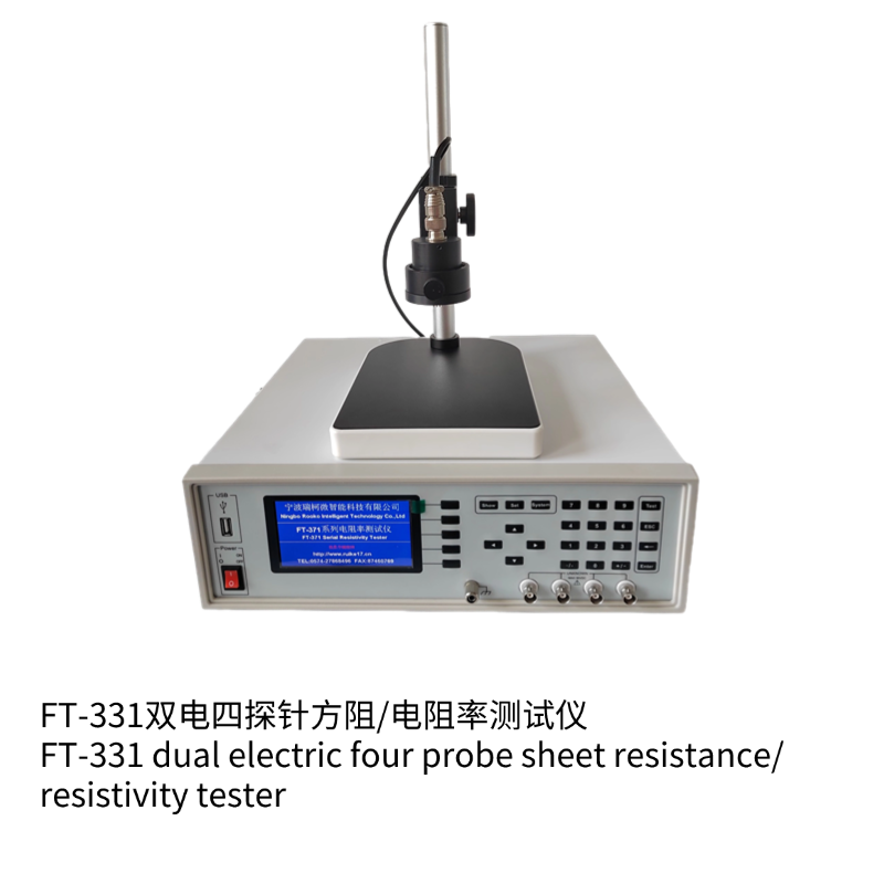
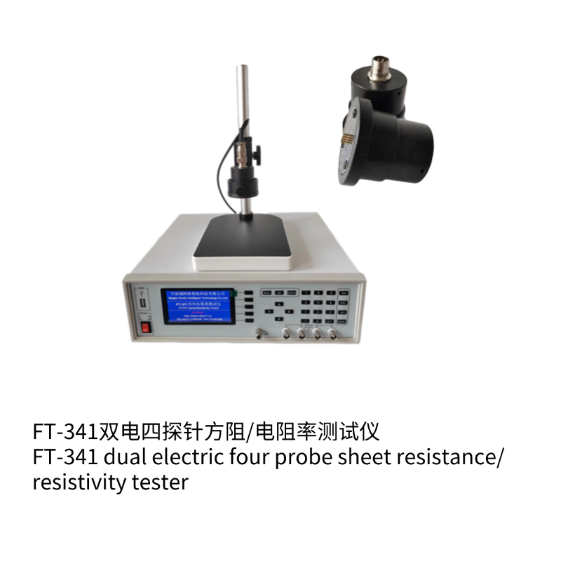
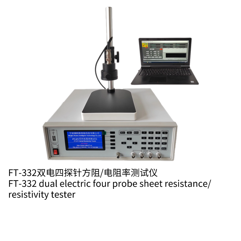
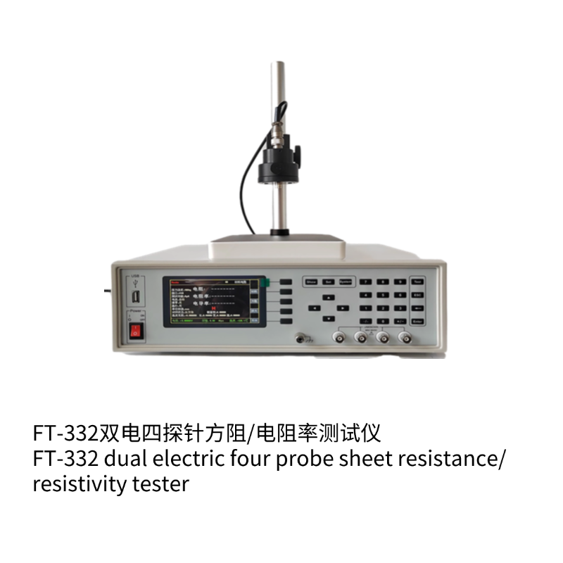
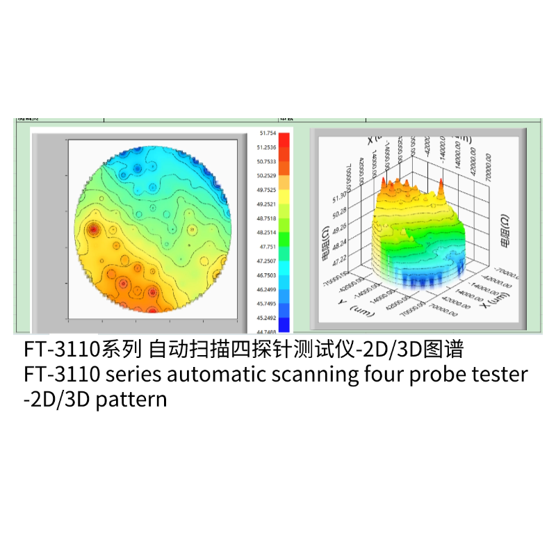
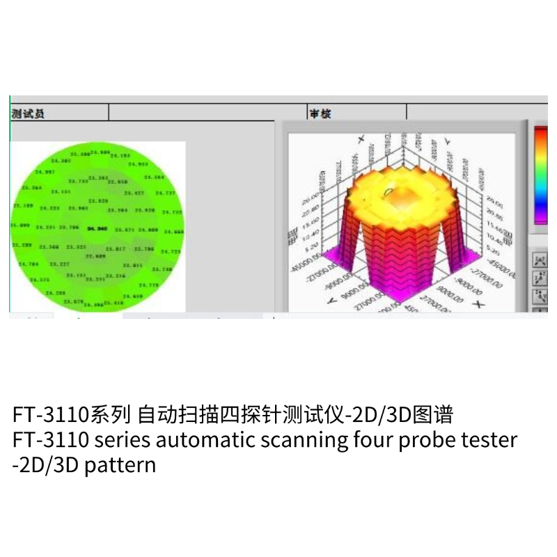
Four-Probe Resistance/Resistivity Tester
Surface and Volume Resistivity Tester for Insulating Materials
Conductor Material Resistivity Tester
High Temperature Resistivity Tester
Voltage Drop Tester


详情描述
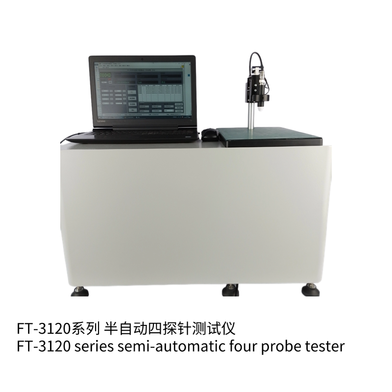
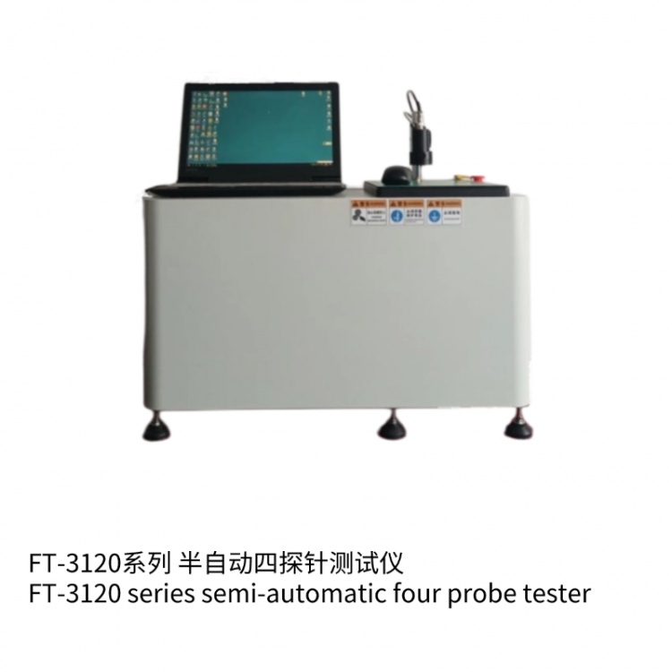
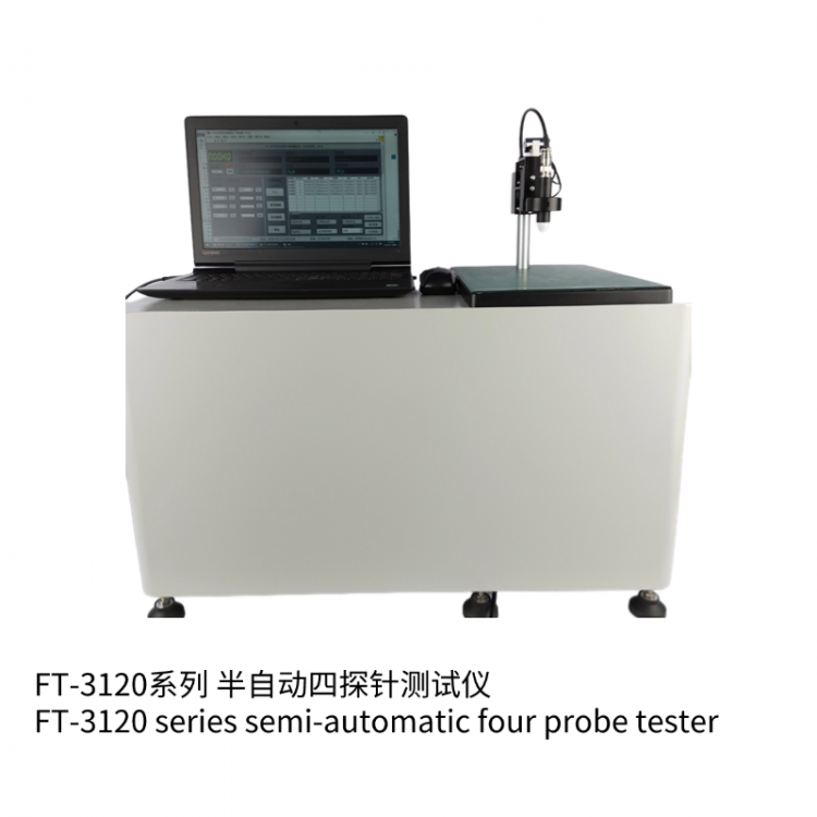
FT-3120B Semi-Automatic Four-Terminal Tester
Function Description: Functionnal description
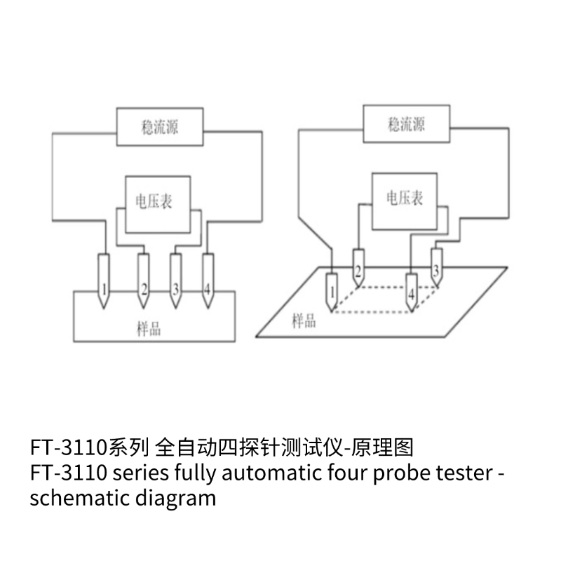
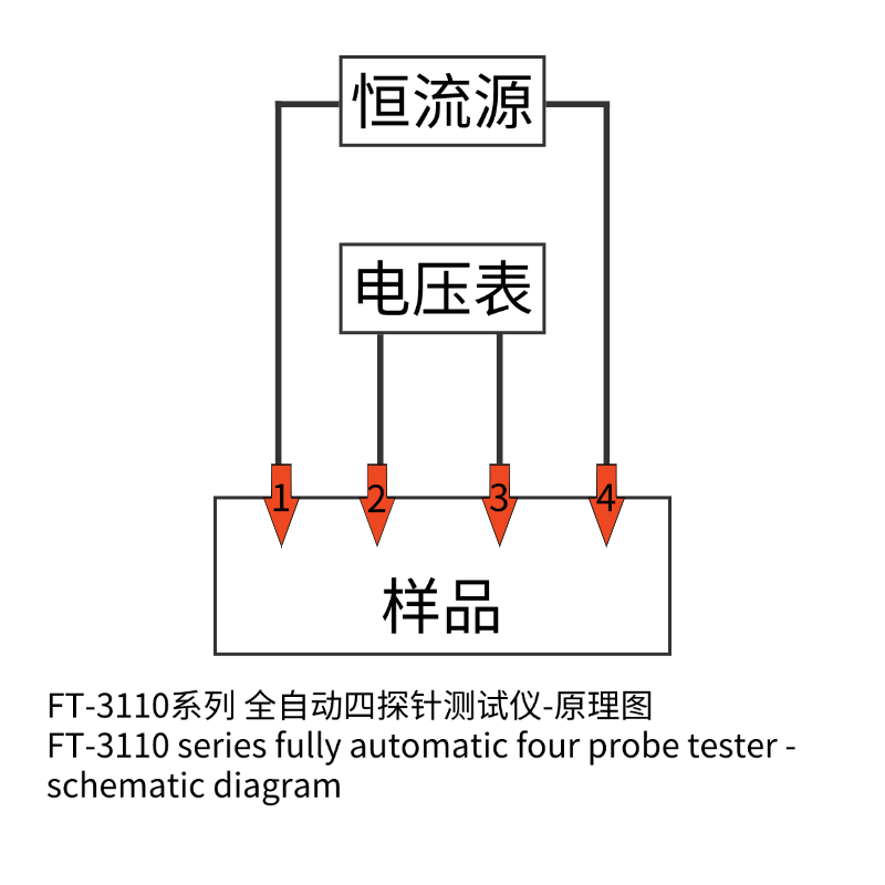
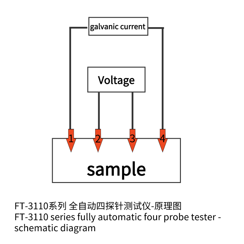
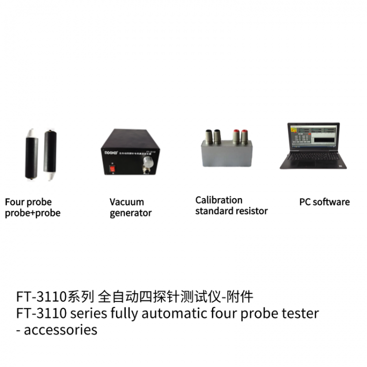
Four-point probe standard testing method, utilizing a stepping system for automatic control of probe contact with the sample, minimizing the impact of human factors on test results; Referenced to A.S.T.M standards; Measures resistance, resistivity, conductivity data, and enables automatic or manual point measurement through PC software data collection and processing; Repeat testing at the same location or multi-point sheet resistance measurement, with data statistical analysis output; Provides standard calibration resistors; Automatic positive/negative current output, automatic positive/negative voltage measurement
Scope of Application
Wafer, amorphous/silicon carbide and conductive film resistivity measurement; selective emitter diffusion wafers; surface passivation wafers; crossbar finger PN junction diffusion wafers; new electrode designs, such as electroplated copper resistance measurement, etc.; semiconductor material analysis, piezoelectric materials, nanomaterials, solar cells, LCDs, OLEDs, touchscreens, etc.
FT-3120B Semi-Automatic Four-Terminal Probe Tester
Technical Specifications
Model and Specifications | FT-3120B |
1.Resistor | 10^-5~2×10^5Ω |
2.Square Resistance | 10^-5~2×10^5Ω/□ |
3.Resistivity | 10^-6~2×10^6Ω-cm |
4.Test Current | 0.1μA.μA.0μA,100µA,1mA,10mA,100mA |
5.Current Accuracy | ±0.1% |
6.Resistance Accuracy | ≤0.3% |
7.PCSoftware Operation | PCSoftware Interface: Resistance, Resistivity, Conductivity, Sheet Resistance, Temperature, Unit Conversion, Current, Voltage, Probe Shape, Probe Spacing, ThicknessData Management Analysis, Large/Low value, mean value, variance, coefficient of variation, sample number, test point count report generation, etc. |
8.Probe Range Selection: | Probe pressure is100-550gBased on sample contact requirements, adjustments are needed. |
9.ExploreNeedle | Insulation Resistance Between Needles: ≥1000MΩ; Mechanical Hysteresis: ≤0.3% Round head copper-plated gold, tungsten steel material, probe spacing1mm;2mm;3mmOptional accessoriesOther specifications are customizable. |
10.Testable Chip Size Selection | Wafer Size:2-12N/A(6Inch150mm,12Inch300mm); Square Sheets: Up to156mm X 156mm Or125mm X 125mm |
11. Analytical Mode | Automatic or Manual Single-point Mode |
12. Pressure Application Method | Measurement Repeatability: Repeatability ≤3% |
13. Protective Functions | Limited range with pressure protection |
14. Test Environment | Lab environment |
15. Power Supply | AC 220V±10%, 50Hz, Power Consumption: <100W |
16. Selection Items | Computers and printers |