Main products include beryllium copper washers, gold-plat...


Product Recommendation
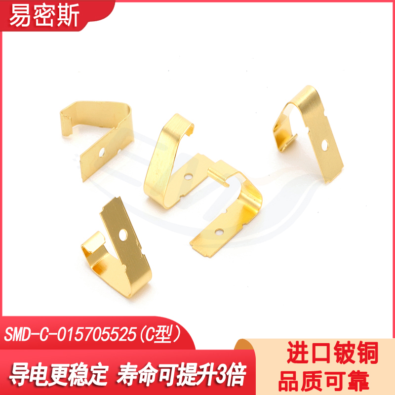
High-elastic beryllium copper spring washer, automotive electronic-specific battery contact strip, PCB contact strip, metal conductive contact strip
Electrical connector-specific 6-lobed spring PCB ground spring metal conductive contact spring available for customization
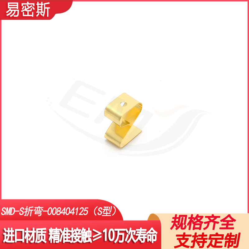
PCB metal conductive spring clip, S-bend type, imported beryllium copper elastic sheet, 0.08*4.0*4.1*2.5MM
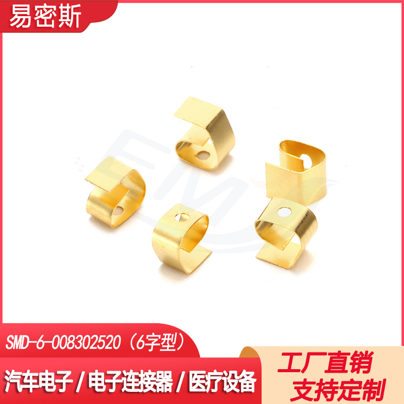
High-elastic beryllium copper spring washer, automotive electronic-specific battery contact strip, PCB contact strip, metal conductive contact strip
Electrical connector-specific 6-lobed spring PCB ground spring metal conductive contact spring available for customization
PCB metal conductive spring clip, S-bend type, imported beryllium copper elastic sheet, 0.08*4.0*4.1*2.5MM
In today's era of increasingly sophisticated and high-power electronic devices, Electromagnetic Compatibility (EMC), thermal efficiency, and structural stability have emerged as the three key factors determining product reliability. As the core of electronic devices, PCBs (Printed Circuit Boards) face severe challenges in their working environment. Against this backdrop, E密斯Contact PadAs a classic and efficient solution, it plays an indispensable role in the electromagnetic shielding and grounding applications of PCBs.
Figure 1: E密斯 Gold Plated Contact Pad
I. Understanding Materials and Their Characteristics
Material Definition:
H62 is a common brass alloy, composed of approximately 60.5% to 63.5% copper (Cu) and the remainder zinc (Zn). This copper-zinc ratio strikes a balance between cost, mechanical properties, and conductivity.
Outstanding balance.
2. Core Features:
Conductive washers' applications on PCBs mainly revolve around two core functions: electromagnetic interference (EMI) shielding and electrical grounding.
Shielding connection between PCB and metal casing/shielding cover:
This is the most common application. At the edges or specific areas of PCBs, there are designated termination areas, usually plated with gold or tin-coated copper foil. H62 conductive spring strips are pre-welded or crimped onto these termination areas.
When the PCB is inserted into the metal housing or covered with a metal shielding cover, the spring is compressed, ensuring a tight metal contact between the housing/shielding cover due to its elasticity, thereby:
2.接地 between modules/sub-boards and the mainboard:
Internally, there may be multiple PCB modules. For instance, a radio frequency module needs to maintain the same reference potential as the mainboard by grounding. Contact pads can be used for grounding connections between two circuit boards, ensuring signal integrity and reducing common-mode interference.
3. Providing grounding or heat dissipation paths for specific components:
For large components requiring individual grounding or heat dissipation, a ground pad can be designed on the PCB beneath them, along with a contact washer. As the component is installed and secured, it will press the washer tightly, creating an additional low-impedance path.
III. Advantages and Limitations Compared to Other Materials
Advantages:
2. Limitations:
Key Considerations for Using Contact Pads in PCB Design
To fully harness the effectiveness of conductive shims, meticulous planning is essential during the PCB design phase.
Ground Pad Design
Pad width should be slightly larger than the contact lead width of the shim to ensure a secure weld.
Surface Treatment: Recommend using Electroless Nickel Immersion Gold (ENIG) or Gold Plating for the best solderability and oxidation resistance. OSP (oxidation prevention) treatment is not suitable for soldering.
2. Installation Method Selection:
SMT Soldering: This is the most mainstream automated installation method. The pads are pre-packaged and precisely placed onto the PCB pads by the SMT machine, followed by welding in a reflow oven. Design must adhere to SMD pad specifications.
Design Standards.
Perforated Welding: Some gasket designs feature pins that can be inserted into PCB through-holes for wave soldering, resulting in higher connection strength; however, the degree of automation is slightly lower.
3. Structural and Design Coordination
Compression Volume and Force: Collaboration with structural engineers is essential to determine the free height of the gasket, the compression volume, and the corresponding contact pressure. Insufficient pressure leads to poor contact, while excessive pressure may cause the gasket to deform permanently or bend the PCB.
The mating surface: The metal housing or shielding cover surface in contact with the gasket should be flat and clean, free of insulating coatings (such as paint, anodized layer) to ensure low impedance contact.
V. Summary and Outlook
E密斯' Contact Shrapnel, with its exceptional comprehensive performance and cost-effectiveness, has emerged as a classic solution for PCB electromagnetic shielding and grounding issues across a broad spectrum of fields, from consumer electronics to industrial control. Although it is not the top-performing,
The material is not the most advanced, yet it remains the "gold standard" that meets the needs of the vast majority of application scenarios.
With the development of 5G, the Internet of Things, and automotive electronics, the requirements for shielding will become increasingly stringent. In the future, contact pads may complement more new materials (such as conductive elastomers, metallized plastics) or surface treatment techniques.
Further optimized in technology and structural design to meet the challenges of higher frequencies, smaller spaces, and harsher environments. However, in the foreseeable future, it will still be an indispensable and reliable tool in the PCB engineer's toolkit.
E密斯 has been specializing in the production of various precision metal shot and beryllium copper spring strips for over 15 years. With deep expertise in material selection, electroplating, and precision stamping, we offer customized bulk services in connector systems and shielding solutions to our clients.


b2b.china9.net © Zhongshang 114 Hebei Network Technology Co., Ltd.Address: Room 6009, Oriental New World Center, No.118 East Zhongshan Road, Qiaoxi District, Shijiazhuang City, Hebei ProvincePlatform Service Hotline: 4006299930