
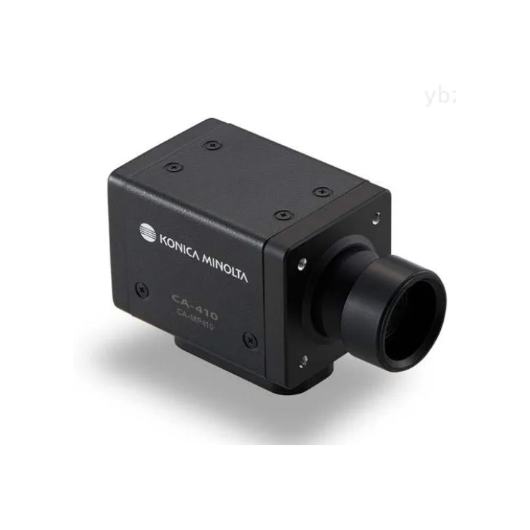
 CA410 Color Analyzer
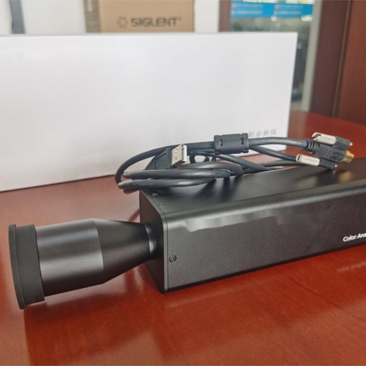 Color Analyzer
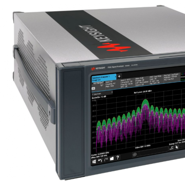 N9030B PXA Signal Analyzer, 2Hz to 50GHz
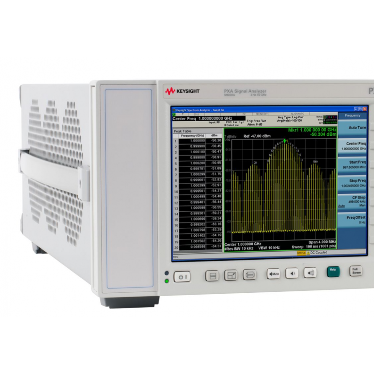 N9030A PXA Signal Analyzer, 3Hz to 50GHz
 N5224B PNA Microwave Network Analyzer
 N5224A PNA Microwave Network Analyzer, 43.5 GHz
 E5071C ENA Radio Frequency Network Analyzer
Product Details
Instrument sales, rentals, maintenance, calibration, and acquisition, caterin...

产品Price 23000.00/Tai
最小起订Quantity:1 Tai 供货总Quantity: 20 Tai


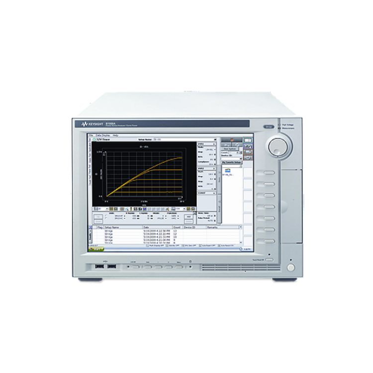
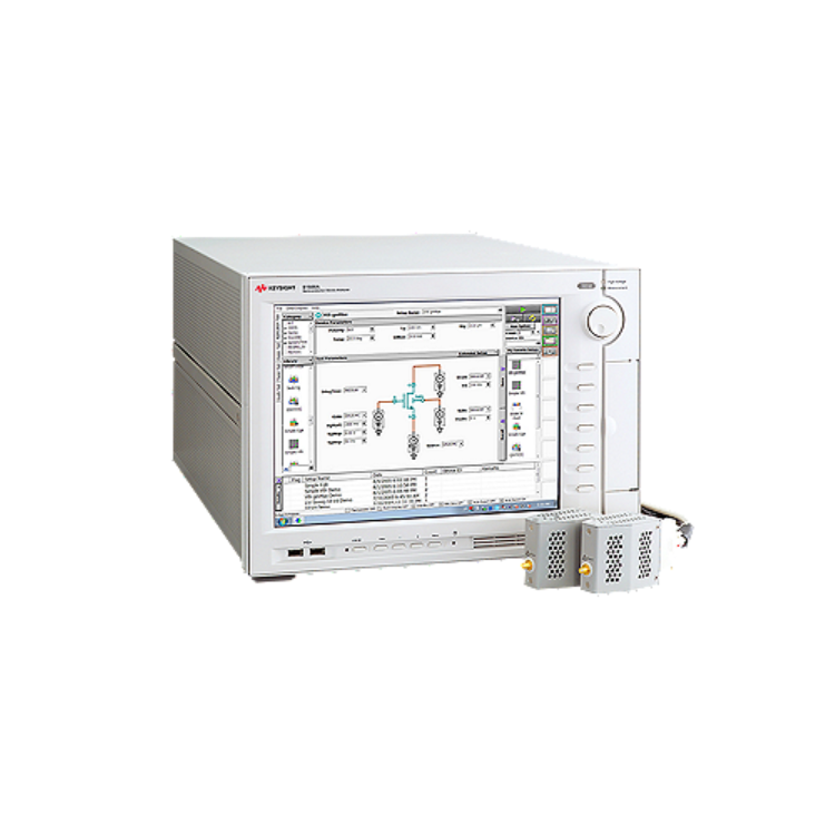
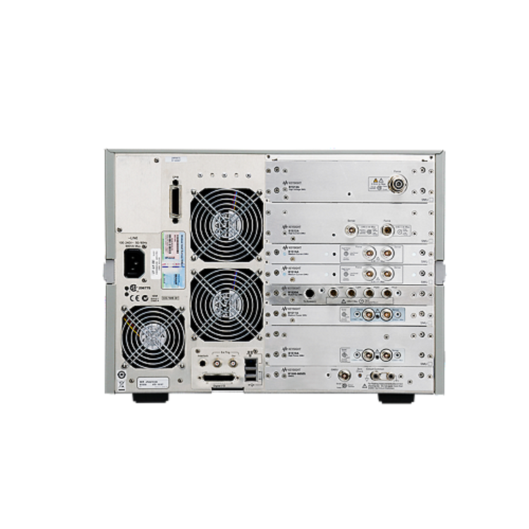
Key Features and Technical Specifications Comprehensive solution for power device characterization, up to 1500 A and 10 kV Medium current measurement and high voltage bias (e.g., 500 mA, 1200 V) μΩ Conductance Resistance Measurement Function At high voltage bias, sub-pA level current measurements can be performed. Automated thermal testing conducted across a temperature range of -50°C to +250°C Comprehensive device measurement capabilities Automatic capacitance measurements (Ciss, Coss, Crss, etc.) can be performed at up to 3000 V DC bias. 10 μs high-power pulse measurement IGBT/FET gate charge measurement on packaged devices and wafers High-voltage/High-current Fast Switching Option, suitable for GaN Current Collapse Effect Characterization Up to 5 high-voltage (3 kV) power/metering channels, offering great flexibility Enhanced measurement efficiency Automatically switch between high-voltage and high-current measurements without the need for re-wiring. Automated test circuit formation for measuring the transistor junction capacitances (Ciss, Coss, Crss, Cgs, Cgd, Cds, etc.) on packaged devices and wafer-level components. Standard test fixtures with interlocking mechanism for packaging power device testing Supports high-power wafer testing up to 200 A and 10 kV Oscilloscope view supports verification of applied voltage and current waveforms MS Windows EasyEXPERT software simplifies the data management and analysis process. Upgradable and scalable hardware architecture A wide range of measurement module options Supports high-power devices with up to 6 connection pins 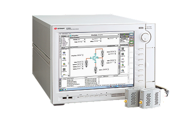

Phone Consultation