


详情描述
Detailed Description:
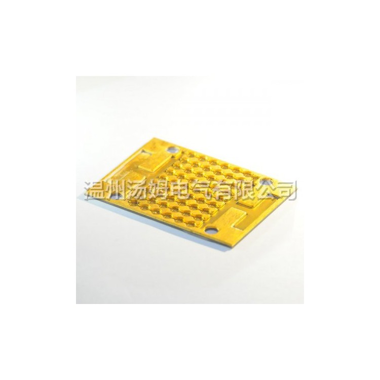
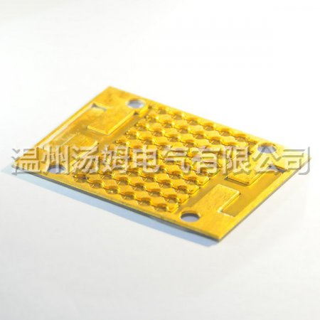
PCB Manufacturing Ceramic Substrate
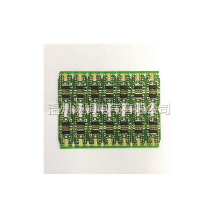
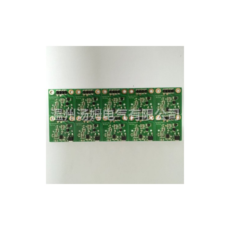
Layer Count: 6 Ply
Board Thickness: 1.6 mm
Base Material Process: Lead-Free Soldering
Surface Treatment: Gold Filled
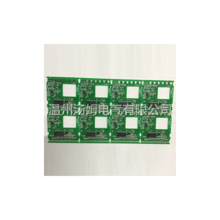
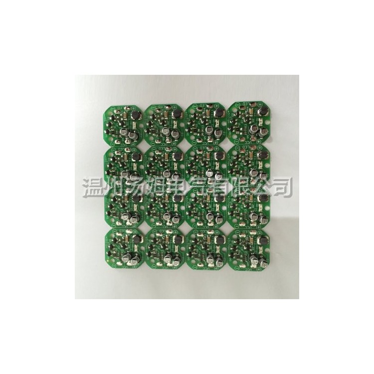
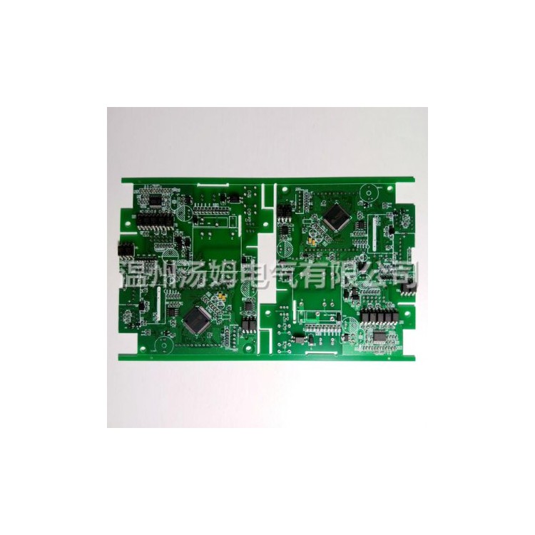
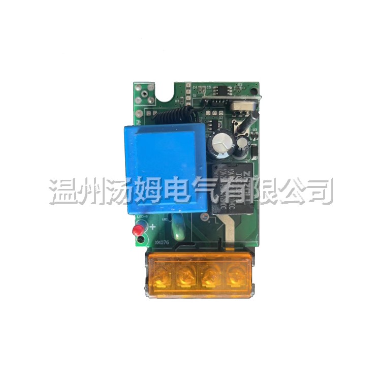
Size: Single Sheet Size 125*53.7MM
These four ceramic substrates are manufactured by FASTPCBA with gold plating finish on the surface. The solder pads are made of ceramic material, featuring ultra-thin composite substrates with excellent electrical insulation properties, high thermal conductivity, superior soft solderability, and high adhesion strength. They can be etched into various patterns like PCBs, offering great current carrying capacity. Our company undertakes manufacturing of PCBA with various processes. If you are interested in these products, please feel free to inquire for pricing!
PCB Ceramic Substrate
High Temperature Co-Fired Multilayer Ceramic Substrate Technology (HTCC)
HTCC is an early-stage technology, which involves first adding alumina or nitride ceramic powder to an organic binder, then mixing it uniformly to form a paste. The paste is then spread into sheets using a scraper, followed by a drying process to form green bodies. Conductive holes are designed for each layer, and wire bonding paste is printed through a screen to route and fill the holes. The green bodies are stacked and sintered in a high-temperature furnace (at 1600℃) to form the alumina ceramic substrate.
However, this technology has obvious drawbacks, as the high sintering temperature restricts the selection of metal conductor materials, usually opting for metals with high melting points but poor conductivity, such as tungsten, molybdenum, and manganese. Additionally, the manufacturing costs are also very high.
2. Low Temperature Co-Fired Ceramic Substrate (LTCC)
Similar to the HTCC technology principle, the improvement lies in lowering the sintering temperature to 850~900°C, which allows for using conductive metals like gold and silver as electrode materials and wiring.
Due to its use of screen printing technology, alignment errors may occur due to webbing issues, and there is also a problem with differential shrinkage ratios when the ceramic layers are sintered together, affecting the yield of finished products. To improve the thermal conductivity of LTCC, thermal or conductive vias can be added in the bonding area, but this will also increase costs.
3. Direct Copper Clad Ceramic Substrate (DBC)
This technology involves the eutectic sintering of ceramic substrates with copper foil at high temperatures (1065°C). The wiring requirements dictate the formation of circuits through etching. Due to the excellent electrical and thermal conductivity of the copper foil, and the ability of alumina to effectively control the expansion of the Cu-Al2O3-Cu composite, the DBC substrate exhibits a thermal expansion coefficient similar to that of alumina.
DBC boasts good thermal conductivity, high insulation, and high reliability. However, due to micro-pores that easily form between the ceramic substrate and Cu layer, it reduces the product's resistance to thermal shock. Additionally, copper foil tends to warp and deform at high temperatures, which is why the thickness of the copper foil on the DBC surface is generally over 100mm. Moreover, due to the use of chemical etching technology, the line width of the DBC substrate patterns is typically over 100mm, making the production technology and costs very high.
4. Direct Copper Plated Ceramic Substrate (DPC)
It involves preliminary cleaning of the ceramic substrate, followed by depositing a Ti/Cu layer as a seed layer on the substrate surface using vacuum sputtering. Next, the circuit is fabricated through photolithography, development, and etching processes. The circuit thickness is then increased by electroplating/chemical plating methods. The substrate is completed after the photoresist is removed.
The advantages include low-temperature manufacturing (below 300℃), which avoids deformation of the material or circuit structure due to high temperatures, and also reduces manufacturing costs. The use of thin-film and photolithography techniques makes the metal circuits on the substrate more precise, making DPC substrates particularly suitable for packaging electronic devices with high alignment accuracy.
The above four ceramic substrate manufacturing technologies each have their unique features. However, under the trend of intelligentization, the application of DPC technology will become more widespread to meet the demand for miniaturization and high precision. Slitong's mature DPC technology can customize 3D-shaped substrates to cater to the diverse needs of users.
询价单


