


- AllProduct Category
-
General Instrument Consumables & Inspection Services
Solar Energy/Semiconductors
Surface Analysis
Element Analysis


详情描述
Product Introduction
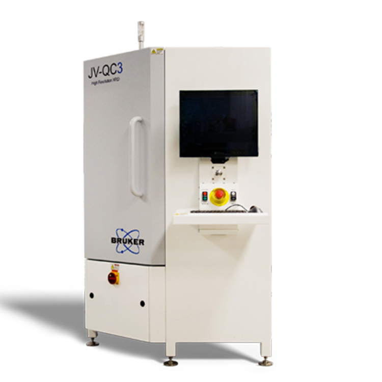
The JV-QC3 is a new semiconductor production quality control device launched by the Brook Semiconductor Division, a high-resolution X-ray diffraction instrument specifically designed for quality control in the compound semiconductor industry.
Brooke Technology Co., Ltd.'s semiconductor department has a history of over 30 years in the research and development of quality control (QC) equipment. The Bede QC200 model, as the predecessor to the QC3, has been widely used globally for testing and production control of semiconductor substrates or epitaxial layers made of Si, GaAs, InP, GaN, and other related materials.
Product Features
Achieved partial or full automation of high-resolution X-ray diffraction testing technology, and can customize dedicated automation control programs and quality control parameters according to the specific requirements of the customer's products.
Automated robotic arms can be configured to meet customer requirements, achieving fully automated loading of semiconductor wafers and executing the testing process on the production line in full automation.
● The system can simultaneously place multiple wafer slices, with a single automated program handling the entire wafer testing process. For instance, with 100mm diameter wafers, up to 4 or more can be placed on the sample tray at once. The control software can sequentially execute the test program menu for all wafers on the tray, thereby reducing manual operation time and enhancing testing efficiency.
Product Advantages
● High-resolution X-ray diffraction for semiconductor materials, without compromising resolution requirements for other X-ray testing techniques.
Compared to the previous generation's quality control equipment, the X-ray intensity has been increased. It achieves higher testing accuracy at the same testing speed; and faster testing speed at the same testing accuracy.
Reduced the purchase and maintenance costs of equipment and accessories.
Lower operating costs.
"XRG Protect" technology, which effectively extends the lifespan of X-ray tubes.
● Eco-friendly green working mode, effectively reducing energy consumption during standby.
● Supplying mechanical arms for automated wafer handling, equipped with simultaneous testing capability for multiple wafer batches, enhancing production testing efficiency.
Operation is simple, no professional staff required.
● Chip alignment, data collection, and analysis are fully automated.
Automated Data Fitting Analysis Software.
● Remote control of data collection and result reporting from the production line is achievable
Technology Application
Direct measurementQuantityAnd confirm multipleLayerExterior membrane structure extensionLayerComponents, RelaxationDegree and adaptability
AutomaticStraightness round slices, automated testing, automated data analysis, automatic output of test results
Automated diffraction data fitting analysis using Bruker JV - RADS software (i.e., Bede RADS)
Achieve X-ray diffraction for symmetric, asymmetric, and oblique-symmetric geometries of compound semiconductor materials


