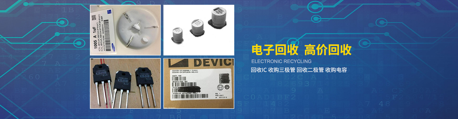


Transistors, also known as semiconductor transistors, bipolar junction transistors, or three-terminal transistors, are semiconductor devices used to control current flow. Their function is to amplify weak signals into larger amplitude electrical signals and are also used as contactless switches.
Transistors are one of the fundamental semiconductor components, known for their current amplification capabilities and serving as the core elements in electronic circuits. A transistor is created by fabricating two closely spaced PN junctions on a single semiconductor wafer, dividing the entire semiconductor into three sections: the middle section is the base region, and the two side sections are the emitter and collector regions. The arrangement can be either PNP or NPN.
Working Principle:
Transistors, commonly referred to as "transistors," are divided into two types based on material: Germanium and Silicon. Each type comes in two configurations: NPN and PNP. However, the ones used are Silicon NPN and Germanium PNP transistors. In the NPN type, "N" stands for Negative, indicating that phosphorus is added to high-purity silicon to replace some silicon atoms, resulting in free electrons for conduction under voltage. In the PNP type, "P" stands for Positive, meaning boron is added in place of silicon to create a large number of holes that facilitate conduction. Both types operate on the same principle, with the only difference being the polarity of the power supply.
A transistor is a current amplifying device, but in practical use, its current amplifying effect is often converted into a voltage amplifying effect through resistors.
Principle of Magnification
1. The emitter region emits electrons towards the base region.
Power supply Ub is applied across resistor Rb to the emitter junction, causing the emitter junction to be forward biased. The majority carriers (free electrons) in the emitter region continuously cross the emitter junction into the base region, forming the emitter current Ie. At the same time, majority carriers also diffuse from the base region to the emitter region, but since the concentration of majority carriers is significantly lower than that in the emitter region, this current can be disregarded. Therefore, it can be considered that the emitter junction is primarily an electron flow.
2. Electron Diffusion and Recombination in the Base Region
As electrons enter the base region, they initially concentrate near the emitter junction, gradually forming a density gradient. Under the influence of this gradient, electrons are driven to diffuse across the base towards the collector junction, where they are swept into the collector region, forming the collector current Ic. A small portion of electrons, due to the thinness of the base, recombine with the holes in the base. The ratio of the diffused electron flow to the recombined electron flow determines the amplification capability of the transistor.
3. Power Zone Collects Electronics
Due to the significant reverse voltage applied to the collector junction, this reverse voltage generates an electric field that prevents electrons from the collector region from diffusing into the base region. Simultaneously, it draws electrons diffusing near the collector junction into the collector region, thereby forming the main collector current, Icn. Additionally, the minority carriers (holes) in the collector region also exhibit drift motion towards the base region, creating a reverse saturation current, denoted as Icbo. Its value is very small, yet it is highly sensitive to temperature.
