
Introduction to UV-Visible Diffuse Reflection
Diffuse light refers to the light emitted from a light source that enters the interior of a sample, undergoes multiple reflections, refractions, scattering, and absorption before returning to the sample's surface. The diffuse reflection spectrum is primarily related to the electronic structure of the material.
For opaque samples such as powdery substances, the direct light system cannot be used to test and further understand their properties. Assistance is required.ScoreballTest diffuse light. Diffuse light is the light formed by the molecular interactions within a sample, carrying rich information about the sample's electronic structure and organization.
Testing samples such as turbid solutions, suspension solutions, and irregularly shaped lenses, if the direct light system is used for testing, light scattering or path deviation may occur as the light passes through the sample, causing changes in the shape and size of the light spot reaching the detector, leading to errors in the test results. To address the inaccuracy caused by path deviation and beam change, it is necessary to adopt...Score BallTo collect, the signal light isScore BallMultiple diffusions can lead to measurement errors. To address inaccuracies caused by light path deviation and beam alteration, an integrating sphere is needed to collect the signal light. Inside the integrating sphere, the light undergoes multiple diffusions and is measured in a constant ratio.
Introduction to Semiconductor Bandgap
Under normal temperatures, semiconductors are materials with conductivity between conductors and insulators, possessing a forbidden energy band. By exciting semiconductor materials with appropriate light, electrons in the valence band can be promoted to the conduction band, creating electron-hole pairs. The energy difference between the bottom of the conduction band and the top of the valence band represents the bandgap size. The energy band structure of semiconductors can be analyzed to understand their photoelectric properties. UV-Vis DRS (Ultraviolet-Visible Diffuse Reflectance Spectroscopy) is a method used to analyze the bandgap value.
An Example of Ultraviolet-Visible Diffusion and Bandgap Calculation
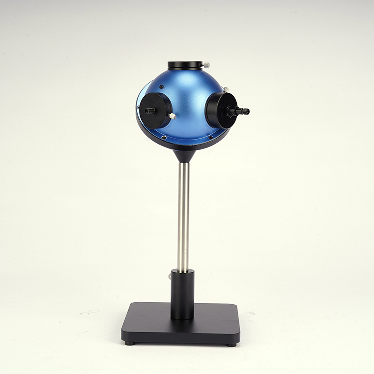
This article takes a powder sample as an example, utilizing the Thermo Scientific UV2600 UV-Vis Spectrophotometer and the IS2600 integrating sphere for testing. The integrating sphere features both positive and negative grooves to accommodate both standard and微量 sample volumes. Additionally, the powder cell is equipped with a quartz window, preventing sample powder from falling into the instrument or integrating sphere and causing contamination.
First, baseline testing was conducted using a standard whiteboard (R% mode), followed by diffuse reflection testing on the samples to obtain their ultraviolet-visible diffuse reflection spectrum.
The diffuse reflection law, also known as the Kubelka-Munk function, reveals:
F (R)=(1- R)2/2 R= K/S
R, K, and S represent the reflectance coefficient, absorption coefficient, and scattering coefficient of the sample, respectively.
Additionally, according to a formula proposed by Tock, Davis, Mott, and others, commonly referred to as the "Tock Formula":
(hρ*α) n= A (hε- Eg)
In these two functions, h is Planck's constant, ρ is the frequency, A is a constant, α is the absorption exponent, and Eg is the semiconductor bandgap width.
Here, n for indirect bandgap semiconductors is n=1/2, and for direct bandgap semiconductors, n=2.
The absorption coefficient α is proportional to F(R∞), and since α can be replaced by F(R∞) in the Tauc equation, it can be transformed into:
[F(R)*hv]n = A(hv - Eg)
Then, Hv is the horizontal coordinate, and (F(R∞)* Hv)^n is the vertical coordinate. When (F(R∞)* Hv)^n equals 0, the corresponding horizontal coordinate Hv is the size of the Eg value. Here's an example of a direct-type semiconductor material:
Example of specific data processing methods:
As per the UV-Vis DRS data (with wavelength as the x-axis and reflectance as the y-axis), as shown in the table below:
This will convert to the data in Column D: hv = 1240/wavelength, units in eV.
Thus, converting a vertical coordinate to F column data results in F(R∞) = (1 - R)² / (2R), where R represents the reflectance value, i.e., the value from column B divided by 100.
Graphs can be obtained from the table data, depicting the x and y axes, and by using the linear extrapolation method, the intersection point with the x-axis represents the Eg value.
Conclusion
The aforementioned example demonstrates the use of the Thermo Scientific UV-2600+ spectrophotometer with the IS2600 integrating sphere to calculate the width limits of semiconductor materials. This is achieved through measurements of the semiconductor materials' diffuse reflection using the UV-2600+ spectrophotometer with the IS2600, which also provide insights into the electronic structure and light absorption properties of the materials.