

Lab-Specific HMDS Oven Critical Role of the Miniature HMDS Processing Furnace
The surface of chip products is typically hydrophilic due to the adsorption of a layer of water from the ambient humidity. To achieve appropriate adhesion for the photoresist, the surface needs to be made more hydrophobic to better match the chemical properties of the photoresist.
Addressing the issue of insufficient adhesion in photoresist
The natural oxidation layer on the product surface: Silicon wafers exposed to air form a SiO₂ layer about 1-2nm thick, which is rich in hydroxyl groups (-OH) and has strong hydrophilicity. Photolithographic resins (especially chemically amplified types) are typically hydrophobic, and during direct spin coating, dewetting occurs due to a mismatch in surface energy, leading to pinhole or island-like defects.
The improvement effect of HMDS: Through surface treatment, the contact angle of the silicon wafer surface is increased from ~40° to 65°-80° (close to the contact angle of photoresist), ensuring uniform spreading of the photoresist and the formation of a continuous film layer. Experiments show that after using HMDS, the adhesion of the photoresist can be increased by 3-5 times, making it less likely to fall off during subsequent development and etching processes.
Enhance the integrity of photolithography patterns
Key Role in Fine Line Technology: Below the 28nm process node, the linewidth of photoresist lines reduces to sub-micron levels, with the edge stress concentration effect intensified. Without HMDS treatment, line collapse (Line Collapse) is highly prone during development. For instance, in 193nm immersion lithography, using HMDS can enhance the anti-collapse capability of 50nm linewidth by 20%.
Optimization of filling for deep holes/groove structures: For devices with high aspect ratios (>20:1) such as 3D NAND, HMDS can reduce the contact angle at the bottom of the holes, preventing void formation and improving graphic transfer quality.
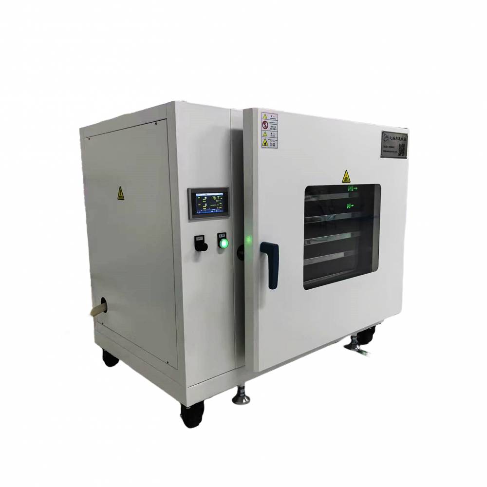
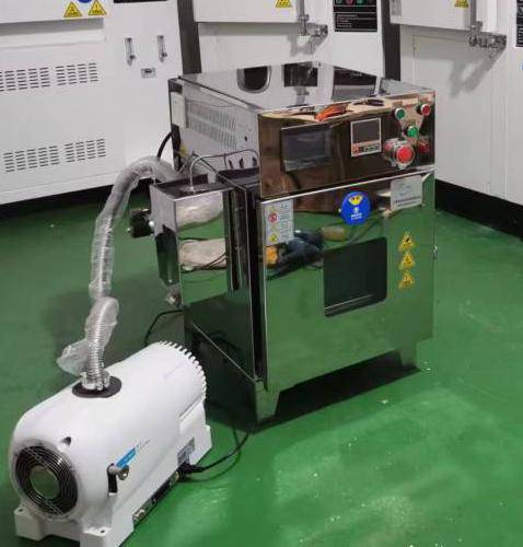
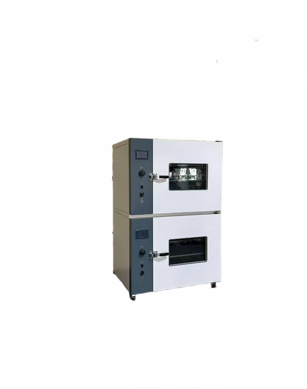
Lab HMDS-Specific Oven Primary Functions of the Small HMDS Treatment Oven
HMDS Coating: Apply HMDS uniformly to the product surface using vapor prime coating.
Curing by baking: Generally baked for 60-500 seconds at 100-150°C to facilitate complete chemical reaction.
Volume: Customizable to 300×300×300 mm (compatible with 2-12 inch products)
Material: Outer case made of high-quality stainless steel, inner case of 316L grade stainless steel.
Temperature Range: RT+20-200℃
Vacuum Level: ≤1 torr
Automation: Color touch screen human-machine interaction, one-touch operation
HMDS Control: Adjustable HMDS Additive Amount
Oil-Free Scroll Vacuum Pump
HMDS Oven Optional Features:
HMDS Leak Alarm Alert Feature
Low Level Alarm Function for HMDS
Process Data Recording Function
Program Lock Protection Features


![]()
