

Deposition Equipment, Anti-Adhesion Vapor Deposition System, Nano Imprint Anti-Adhesion Equipment Background
Nanoimprint technology employs a physical contact method for graphic transfer, achieving high resolution with the minimum resolution less than 5 nanometers. Substrates can be reused multiple times, significantly reducing production costs and effectively improving efficiency. As a promising next-generation lithography technology, nanoimprint technology boasts a range of advantages such as low cost, good reproducibility, and strong controllability, and is gradually being applied in various fields of microfabrication. Since imprinting is performed on microstructures, friction and the resulting demolding are critical factors affecting the quality of imprinting.
脱模: demolding
Demolding refers to the process of separating the wafer from the mother mold. After demolding, the complete grating structure is left on the wafer.
Surface modification of the template used in the nanoscale imprinting technique with octyltrichlorosilane, the process and chemical mechanism of forming a monomolecular film on the template surface via vapor phase deposition, and the template with surface modification can significantly reduce the interaction force between the template and the imprinting polymer layer, achieving better transfer and replication during the nanoscale imprinting process.

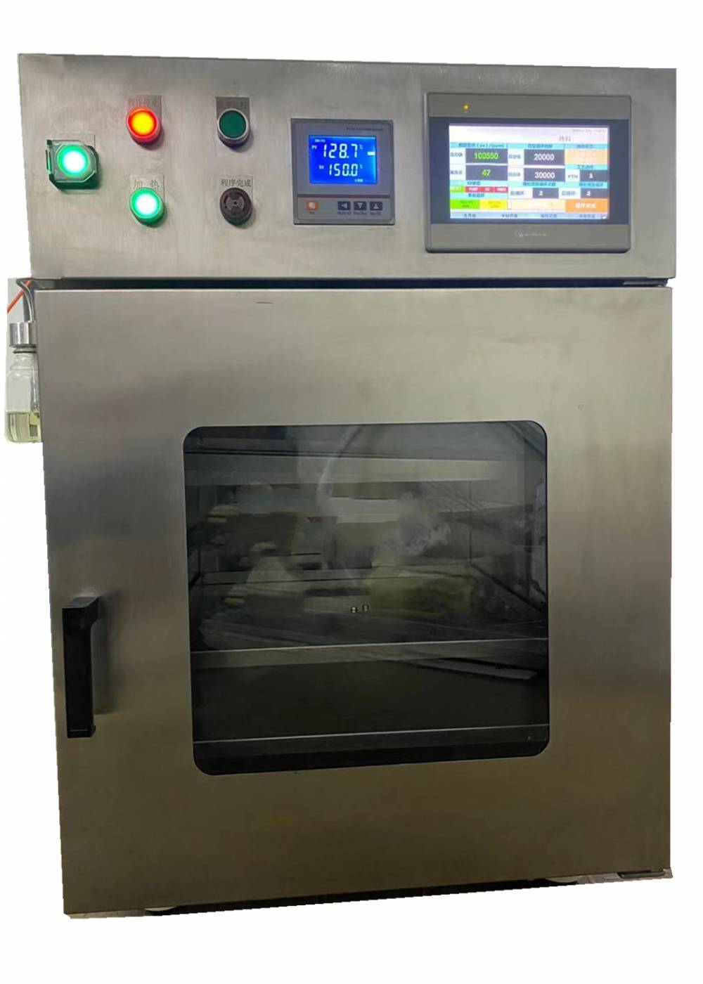
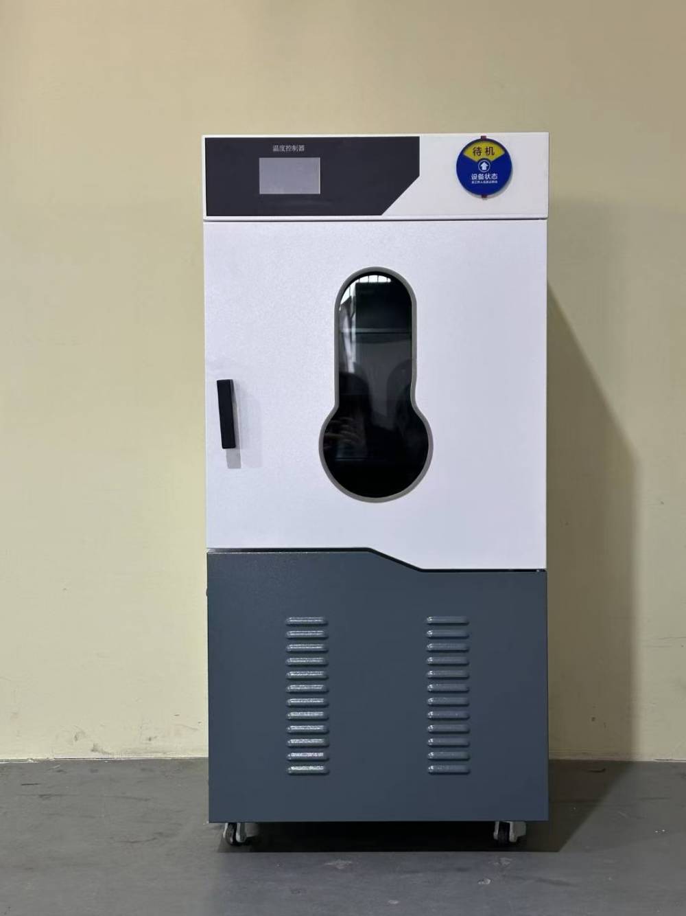
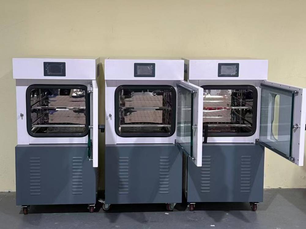
Deposition Equipment, Anti-adhesive Vapor Deposition System, Core Components for Nanoimprint Anti-adhesive Equipment
Airline System: N2, and delivery of other reaction gases.
Reaction chamber: Made of high-temperature and corrosion-resistant materials, equipped with a heater.
Vacuum System: Maintains low-pressure environment, down to below 1Torr.
Exhaust Treatment Device: Processes unreacted substances (due to flammability and explosiveness, requiring combustion or adsorption neutralization).
Control System: Human-Machine Interface for monitoring parameters such as temperature, pressure, gas flow, etc.
Temperature Control System: RT-200℃ High Precision Daily Temperature Controller + RSS Loop, Overheat Protection Device
Safety System: Integrated with an automatic refilling system and a microcomputer temperature control module, it achieves full-process automation of vacuum extraction, nitrogen displacement, and temperature control. The one-touch operation interface supports multi-group program storage, meeting the differentiated processing requirements for wafers ranging from 2 inches to 12 inches.
Deposition Equipment, Anti-Adhesion Coating Evaporation System, Nano Imprint Anti-Adhesion Equipment Applications

Semiconductor Manufacturing: Deposition of dielectric layers (such as SiO₂, SiNx), passivation layers, or isolation layers.
Photovoltaic industry: Absorber or passivation layers for amorphous silicon/microcrystalline silicon thin-film solar cells.
Display Technology: Insulating layer or passivation film used in TFT of TFT-LCD or OLED displays.
MEMS devices: Structural or protective layers for microelectromechanical systems
Nanoimprint: Release Agent Deposition
Biochip: Adhesive Deposition
New Materials: Nanoceramic Materials, Surface-Modified Porous Carbon Composites
Optical Glass: Adhesive Deposition
Shanghai Junsi Instruments, a semiconductor equipment manufacturer, offers vapor deposition equipment including adhesives (e.g., HMDS), anti-adhesive deposition, mold release (PFTS) deposition, and surface modification treatments. We provide precision hot plates, HMDS pre-treatment system ovens, intelligent HMDS vacuum pre-treatment system ovens, MSD ultra-low humidity ovens, cleanroom ovens, clean ovens, nitrogen ovens, oxygen-free ovens, dust-free oxygen-free ovens, vacuum ovens, vacuum storage cabinets, ultra-low temperature test chambers, and ultra-low humidity test chambers, among other environmental reliability equipment.
