

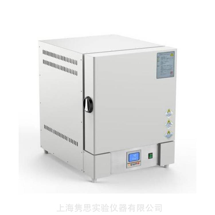

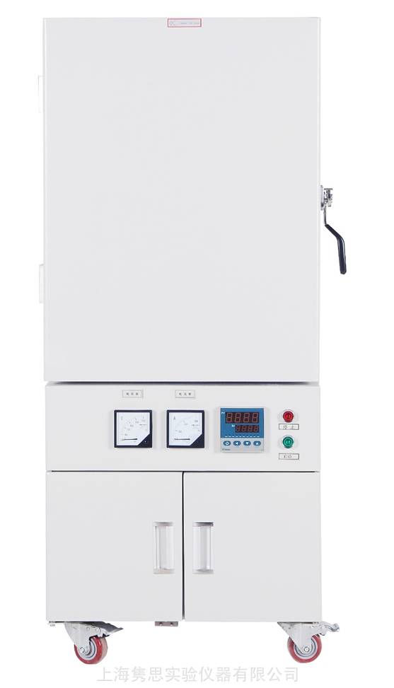
HMDS-Specific Oven, HMDS Vacuum Coating System, Mini HMDS OvenPerformance:
Coating Method: Vapor Deposition
Operating Temperature: RT+50-200℃
Vacuum Level: ≤1 torr
Material of Equipment: Inner case made of 316L stainless steel
Operation Method: One-click operation, automatically completes the process, with an end beep sound.
Dimensions: 450*450*450mm
Compatibility: 2-12-inch wafers and squares, etc.
Vessel for Storage: HMDS Capacity 1000ml
Vacuum Pumps: Imported Dry Vacuum Pumps
Data Processing: Storage of multiple process formulas, utilization of data records
Protective Device: Low-Level AlarmHMDS Leak AlarmOver-temperature protection and heating disconnection, leakage protection, etc.
HMDS-Specific Oven HMDS Vacuum Coating System Compact HMDS OvenUtilize the industry
MEMS, filters, amplifiers, power devices, wafers, glass, precious metals, SiC (silicon carbide), GaN (gallium nitride), ZnO (zinc oxide), ZnS (zinc sulfide), GaO (gallium oxide), diamond, and other third-generation semiconductor materials.
SiC Silicon CarbideHMDS Pretreatment SystemA compound semiconductor material composed of carbon and silicon elements, ideal for manufacturing high-temperature, high-frequency, high-power, and high-voltage devices.
The core advantages of silicon carbide raw materials are:
(1) High-pressure resistance: Lower impedance, wider bandgap, capable of handling greater currents and voltages, leading to smaller product designs and higher efficiency.
(2) High Frequency Tolerance: SiC devices do not exhibit current tailing during the turn-off process, effectively improving the switching speed of the component (about 3-10 times faster than Si), suitable for higher frequencies and faster switching speeds.
(3) High-Temperature Resistance: SiC has a higher thermal conductivity than silicon, allowing it to operate at higher temperatures.
Compared to traditional silicon materials (Si), SiC has a bandgap three times wider than silicon, a thermal conductivity four to five times higher, a breakdown voltage eight to ten times that of silicon, and an electron saturation drift velocity two to three times greater than silicon.
Silicon carbide wafers are used in Schottky diodes, MOSFETs, IGBTs, etc., primarily for infrastructure such as electric vehicles, photovoltaic power generation, rail transportation, data centers, and charging. They are mainly applied in 5G communication, vehicle communication, applications, data transmission, and aerospace.
