

Niobium lithium boasts excellent photoelectrical properties and, as an integrated photonics platform, has garnered extensive attention. On this foundation, various functional photonic devices, such as electro-optical modulators and nonlinear wavelength converters, have demonstrated remarkable performance. Simultaneously, laser devices and amplifiers based on niobium lithium thin films, as critical components of integrated photonic systems, have achieved a series of exciting breakthroughs and advancements.
Niolite materials will lead the revolution in on-chip photonic integrated circuits. Driven by the global digitalization trend, the construction of smart cities and data centers is closely related to the research, development, and production of photonic chips. Niolite materials can be used to manufacture key photonic devices such as integrated lasers, amplifiers, frequency converters, electro-optical modulators, and photodetectors, promoting the rapid development of optical communications, LiDAR, particle sensing, and information processing. In the future, more types of high-integration, multi-functional LNOI chips will enter the industrialization phase, and the on-chip photonic integrated circuit field will also welcome new development opportunities in the digital economy era.
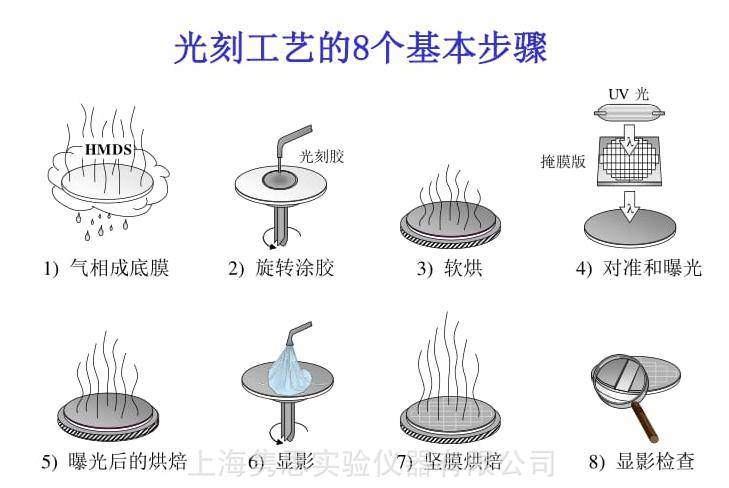
HMDS Pretreatment System Intelligent HMDS Vacuum Oven for Ultra-thin Lithium-Niobium Materials Application
After HMDS vapor deposition on the surfaces of silicon wafers, niobium lithium, silicon carbide, glass, sapphire, gold-plated wafers, and other materials in semiconductor manufacturing, system heating can cause a reaction to generate compounds mainly consisting of siloxanes. It successfully converts the silicon wafer surface from hydrophilic to hydrophobic, and its hydrophobic base can combine well with photoresist, serving as a coupling agent.
HMDS Pretreatment System, Intelligent HMDS Vacuum Oven for Ultra-thin Lithium-Niobium Materials ApplicationTechnical Performance:
Internal dimensions: 300×300×300, 450×450×450, 550×550×550 (mm) (Customizable)
Temperature Range: RT+50-200℃
Vacuum Level: ≤1 torr
Control Method: Human-Machine Interface, One-Touch Operation
Oil-Free Scroll Vacuum Pump

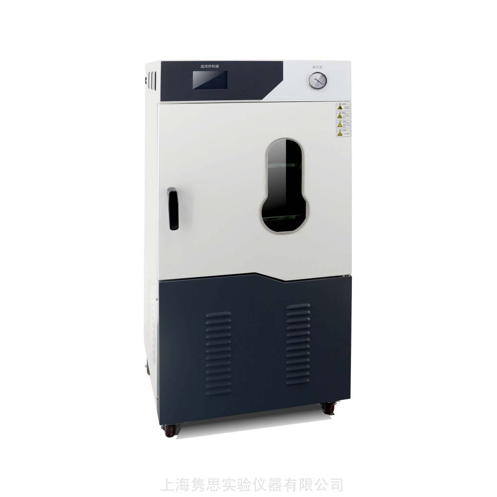
HMDS Pretreatment System, Intelligent HMDS Vacuum Oven for Ultra-thin Lithium-Niobium Material Applications(JS-HMDS90-AI) Features:
HMDS Leaking ReportAlarm alert function
HMDS Low-Level Alarm Alert Function
Process Data Recording Feature
Pipe preheating function
Program Lock Protection Features
