

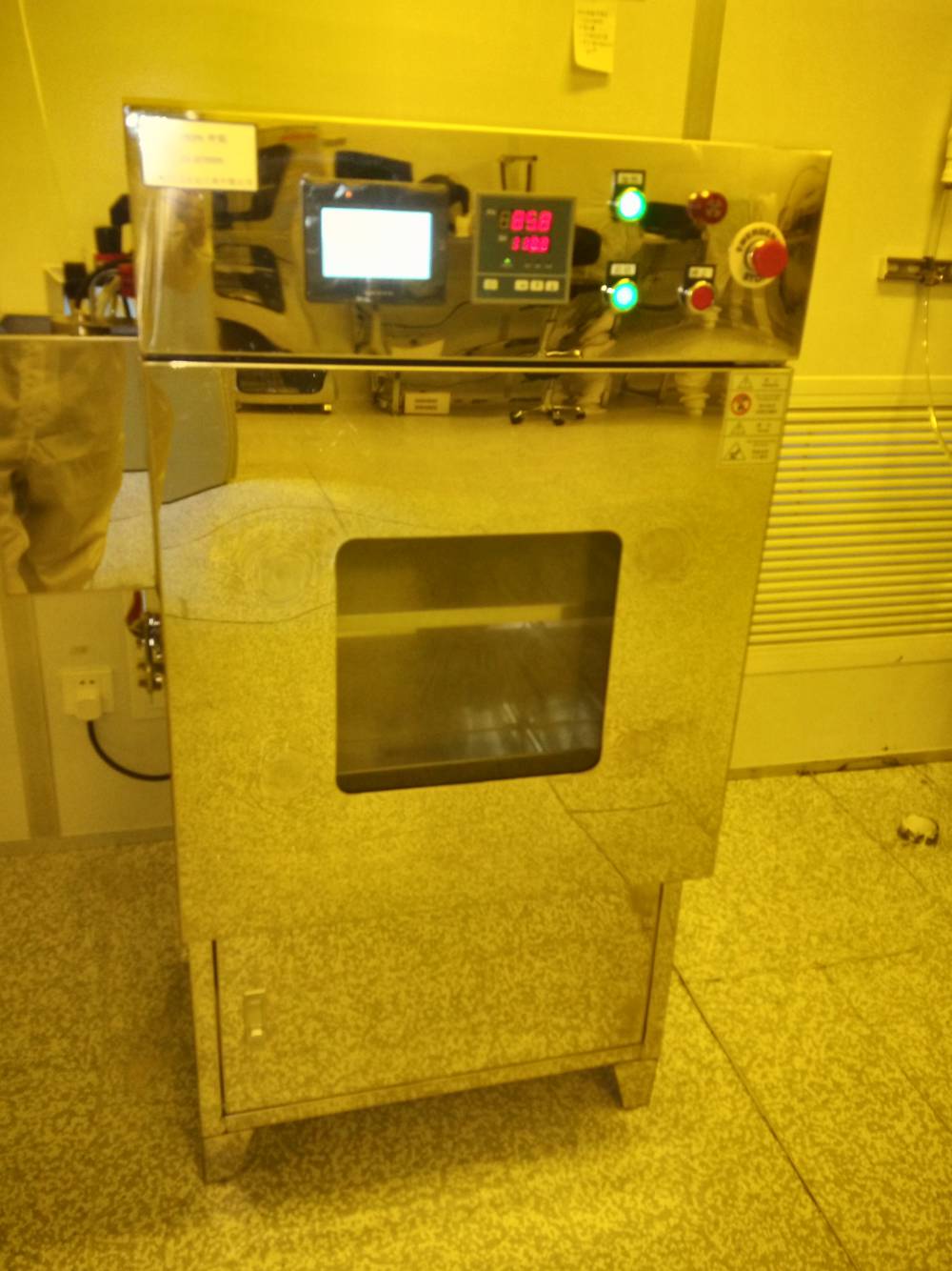
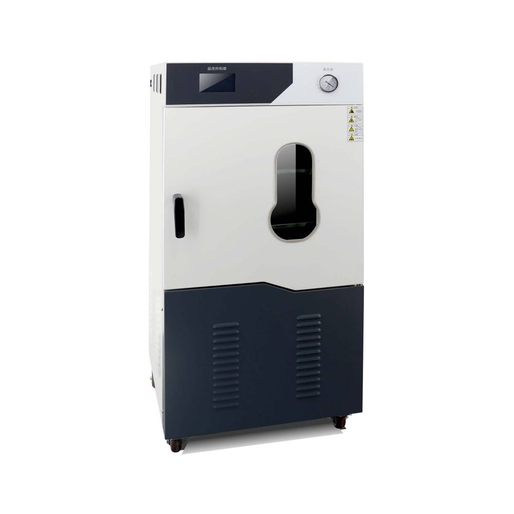
Masked HMDS Vacuum Ovens Light Shield HMDS Ovens HMDS Pretreatment OvenApplication Principle
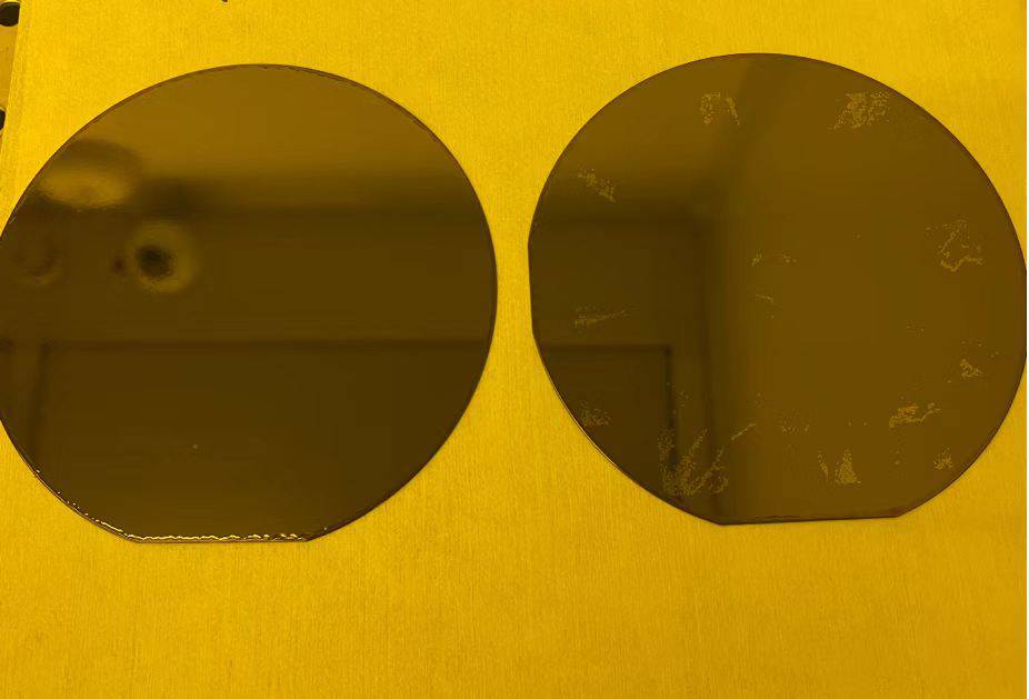
Photomask, also known as a light mask, photomask, or photolithography mask, is a master pattern used in the photolithography process for microelectronics and integrated optoelectronics manufacturing. It consists of an opaque light-blocking film forming a mask pattern on a transparent substrate, which is then transferred onto a wafer through exposure.
Masks are designed with clear and dark fields, and their exposure to photoresist (positive or negative) can be selected based on process requirements. As mentioned earlier, the exposed area of positive photoresist dissolves, while the negative resist does the opposite.
Mask blanks are primarily composed of two parts: the substrate and the light-blocking film. Substrates are categorized into resin substrates and glass substrates, with glass substrates mainly including quartz substrates and soda-lime substrates. Depending on the type of light-blocking film, they can be divided into rigid light-blocking films and latex.
Masking Plate HMDS Vacuum Oven, Light Shield HMDS Oven, HMDS Pretreatment OvenFeatures
Material: Inner box made of 316L grade stainless steel
Process Temperature: 100-150℃
Temperature Resolution: 0.1℃
Temperature Fluctuation: ≤±0.5
Vacuum Level: ≤133 Pa (1 Torr)
Operation Interface: Human-Machine Interface, One-Click Operation
Number of Layers: 1-2
HMDS Control: Additive amount of HMDS can be controlled
Image Processing: Image Inversion
Vacuum pump: Oil-free imported pump
Protective Devices: Emergency Stop, HMDS Leak Alarm, Low HMDS Level Alarm, Overheat Protection, Leaking Protection, Overheating Protection, etc.
Masking Plate HMDS Vacuum Oven, Light Shield HMDS Oven, HMDS Pretreatment OvenConverts the base surface from hydrophilic to hydrophobic, enhancing surface adhesion (HMDS - Hexamethyl Disilazane). Suitable for materials such as silicon wafers, indium phosphide, ceramics, stainless steel, niobium lithium, glass, sapphire, and wafers.
