
A stabilized voltage supply is an electronic device that provides a stable AC or DC power supply to the load, encompassing two main categories: AC stabilized voltage supplies and DC stabilized voltage supplies. When there are momentary fluctuations in the grid voltage or the load, the stabilized voltage supply compensates the voltage amplitude at a response speed of 10-30ms, maintaining stability within ±2%.
Understanding what a voltage regulator is, let's now delve into what a linear voltage regulator and a switching power supply are. What are the differences between the two?
Comparison Analysis of Linear and Switching Voltage Regulators
Based on the operating status of the adjustment tube, we commonly categorize voltage regulators into two types: linear voltage regulators and switching voltage regulators.
Linear voltage regulators refer to power supplies where the regulating tube operates in a linear state. In contrast, switch-mode power supplies operate differently; the switching tube (in switch-mode power supplies, we typically refer to the regulating tube as the switching tube) operates in two states: on – with very low resistance; off – with very high resistance.

A switching power supply is a relatively new type of power supply, offering high efficiency, light weight, the ability to step up or down voltage, and high output power. However, due to the circuit operating in a switching state, it generates significant noise. Let's briefly discuss the working principle of a step-down switching power supply with the illustration below. As shown, the circuit consists of switch K (actually a transistor or field-effect transistor in a real circuit), flyback diode D, energy storage inductor L, and filter capacitor C. When the switch is closed, the power supply supplies power to the load through switch K and inductor L, storing some electrical energy in inductor L and capacitor C.
Due to the self-inductance of inductor L, the current increases slowly after the switch is closed, meaning the output cannot immediately reach the supply voltage. After a certain period, the switch is opened, and due to the self-inductance effect of inductor L (which can be thought of as an inertia-like action of the current in the inductor), the current in the circuit remains unchanged, continuing to flow from left to right. This current flows through the load, returns through the ground wire, to the positive terminal of the flyback diode D, passes through diode D, and returns to the left end of inductor L, thereby forming a loop. By controlling the time the switch is closed and opened (i.e., PWM - pulse width modulation), the output voltage can be controlled. If the on/off time is controlled by detecting the output voltage to maintain a constant output voltage, this achieves the purpose of voltage stabilization.
During the on-off cycle, the inductor stores energy; during the off period, the inductor releases energy, hence the inductor L is called the energy storage inductor. Diode D provides a current path to the inductor L during the off period, so diode D is known as the freewheeling diode.
In practical switching power supplies, the switch K is replaced by a transistor or a field-effect transistor. When the switch is open, the current is very low; when the switch is closed, the voltage is also low, resulting in a very small power dissipation of U x I. This is why switching power supplies are highly efficient.
After reviewing two FAQs about power supplies, you may still be unclear about the calculation of power supply efficiency. In the following FAQs, we will specifically introduce this topic.
Commonly used chips for switching power supplies include: TL494, LM2575, LM2576, LM2596, 34063, 51414, and so on.
Based on the operational status of the regulating tube, we commonly categorize voltage regulators into two types: linear voltage regulators and switching voltage regulators. Additionally, there is also a small power supply that utilizes voltage regulators.
The linear voltage regulator being referred to here is a DC voltage regulator where the regulating tube operates in a linear state. Operating in a linear state can be understood as follows: RW (refer to the analysis below) is continuously variable, i.e., linear. In contrast, in switching power supplies, the switching tube (in switching power supplies, we generally refer to the regulating tube as the switching tube) operates in two states: on - with very low resistance; off - with very high resistance. Tubes operating in a switching state are clearly not in a linear state.
Linear voltage regulators are one of the earliest types of DC voltage regulators used. The characteristics of linear voltage regulated DC power supplies include: the output voltage is lower than the input voltage; they have a fast response time with minimal output ripple; low noise generation during operation; lower efficiency (which is why LDOs, commonly seen today, were developed to address efficiency issues); and significant heat generation (especially in high-power supplies), indirectly adding thermal noise to the system.
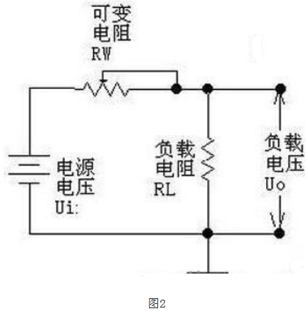
Operation Principle: We first illustrate the principle of voltage regulation in a linear voltage regulator using the following diagram. As shown in the diagram below, a variable resistor RW and a load resistor RL form a voltage divider circuit, with the output voltage being:
Uo = Ui * TImes; RL / (RW + RL), thus adjusting the size of RW can alter the output voltage. Please note that in this equation, if we only consider the value change of the adjustable resistor RW, the output of Uo is not linear. However, if we consider both RW and RL together, it becomes linear. Also, be aware that our diagram does not show the RW terminal connected to the left, but rather to the right. Although this makes no difference in the formula, placing it on the right accurately reflects the concepts of "sampling" and "feedback"---in reality, most power supplies operate in sampling and feedback modes, with feedforward methods being used rarely, or if used, only as auxiliary methods.
Let's continue: By replacing the variable resistor in the diagram with a transistor or a field-effect transistor, and by controlling the size of the "variable resistor" through the detection of the output voltage, we can maintain a constant output voltage. This transistor or field-effect transistor is used to adjust the size of the voltage output, hence it is called an adjustment transistor.
As shown in Figure 1, due to the voltage regulator being串联 between the power supply and the load, it is called a series-type voltage regulator. Correspondingly, there is also a parallel-type voltage regulator, which involves connecting the voltage regulator in parallel with the load to adjust the output voltage. A typical example of a parallel voltage regulator is the TL431 reference voltage regulator. The term "parallel" refers to, as in the voltage regulator in Figure 2, ensuring the stability of the emitter voltage of the attenuation amplifier through分流. While this diagram may not immediately reveal its "parallel" nature, upon closer inspection, it indeed is. However, please note that the voltage regulator here operates in its non-linear region, so if you consider it as a power source, it is a non-linear power source. To facilitate understanding, we will find an appropriate diagram later to illustrate this until it becomes clear and straightforward.
Since a tuning tube is equivalent to a resistor, it generates heat when current flows through it, resulting in a significant amount of heat being produced in a tuning tube operating in a linear state, which leads to inefficient performance. This is a major drawback of linear voltage regulators. For a more detailed understanding of linear voltage regulators, please refer to textbooks on analog electronic circuits. Here, our main goal is to clarify these concepts and their relationships.
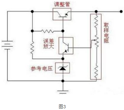
Generally, a linear voltage regulator is composed of several basic components, including an adjusting tube, reference voltage, sampling circuit, and error amplification circuit. Additionally, it may also include parts such as protective circuits and startup circuits. The image below is a relatively simple diagram of the principle of a linear voltage regulator (schematic, with elements like filter capacitors omitted). The sampling resistor takes a sample of the output voltage, compares it with the reference voltage, and the error amplification circuit then amplifies the comparison result to control the conduction degree of the adjusting tube, thereby maintaining a stable output voltage.
Common linear voltage regulator ICs include: the 78XX series (positive voltage type), 79XX series (negative voltage type) (in actual products, XX is represented by a number; the output voltage is equal to the number. For example, 7805 outputs 5V); LM317 (adjustable positive voltage type), LM337 (adjustable negative voltage type); 1117 (low dropout type, with various models, voltage values are indicated by the tail number. Such as 1117-3.3 for 3.3V, 1117-ADJ for adjustable type).
1. DC to DC includes boost (boost-up), buck (buck-down), and BoostThe CK (boost/buck) and inverse structure feature high efficiency, high output current, and low quiescent current. As integration levels rise, many new DC-DC converters require only inductors and filter capacitors for their peripheral circuits; however, these power controllers exhibit significant output ripple and switching noise, and are relatively expensive.
2. LDO: The outstanding advantages of the low dropout linear voltage regulator are its low cost, low noise, and low quiescent current. It also requires minimal external components, typically only one or two bypass capacitors. The new LDO can achieve the following specifications: 30μV output noise, 60dB PSRR, 6μA quiescent current, and a dropout voltage of 100mV. The primary reason the LDO linear regulator can achieve these characteristics is due to the use of a P-channel field-effect transistor in the internal compensation element, as opposed to the PNP transistor commonly used in linear regulators.
The P-channel field-effect transistor does not require base current to drive, thus significantly reducing the power current of the device itself. On the other hand, in the structure using PNP transistors, to prevent the PNP transistor from entering saturation and reducing the output capability, it is necessary to maintain a large input-output voltage difference. The voltage difference of the P-channel field-effect transistor is roughly equal to the product of the output current and its conductance resistance, with a smaller conductance resistance resulting in a very low voltage difference. When the input and output voltages in the system are close, LDO is an excellent choice, achieving high efficiency. Therefore, in applications converting lithium-ion battery voltage to 3V, LDO is mostly used, even though ten percent of the battery's post-discharge energy is not utilized. Nevertheless, LDO can still provide a longer battery life in a low-noise structure.
The Difference Between Linear and Switching Power Supplies
Switched-mode power supplies achieve voltage transformation and stabilization by converting DC to high-frequency pulses and then using electromagnetic transformation. Linear voltage regulators directly串联 a controllable adjustment element to divide the input DC voltage, thereby accomplishing voltage transformation and stabilization, essentially equivalent to串联ing a variable resistor.
Switching voltage regulators offer high efficiency and can step up or step down voltage. Linear voltage regulators can only step down voltage and have lower efficiency. Switching voltage regulators produce high-frequency interference, whereas linear voltage regulators do not. Each has its own advantages and disadvantages.
