
I. Introduction
Regarding operational amplifiers, in electronic circuits, they are typically combined with feedback networks to form certain functional modules, featuring unique coupling circuits and feedback. Their output signals can be addition, subtraction, differentiation, integration, or other operations of the input signals. Initially used in analog computers for mathematical operations, they are now widely applied in the electronics industry as precision AC/DC amplifiers, active filters, oscillators, and voltage comparators.
1.1 Integrated Operational Amplifier
1.1.1 Evaluation Analysis
Integrated operational amplifiers are one of the widely used devices in analog integrated circuits. In various systems, the performance requirements for operational amplifiers differ due to varying application needs.
In the absence of specific requirements, it's advisable to opt for general-purpose integrated operational amplifiers, as this reduces costs and facilitates easy replacement. When multiple operational amplifiers are used in a system, it's best to utilize as many operational amplifier integrated circuits as possible. For instance, the LM324 and LF347 both typically integrate four operational amplifiers into a single circuit.
The evaluation of integrated operational amplifiers depends on their overall performance. The degree of integration is generally measured by the quality factor K, which is defined as: where SR is the conversion rate, measured in V/ms. The higher this value, the better the AC characteristics of the operational amplifier; the input bias current of the amplifier is lib, measured in nA; VOS is the input offset voltage, measured in mV. The smaller the values of Iib and VOS, the better the DC characteristics of the operational amplifier. Therefore, for circuits amplifying AC signals like audio and video, choosing an op-amp with a high SR is preferable; for circuits processing weak DC signals, high-precision operational amplifiers are more suitable (with smaller offset currents, offset voltages, and temperature drifts).
When selecting an operational amplifier, factors other than the quality factor coefficient K should be considered. For instance, whether the signal source is a voltage or current source; the nature of the load, whether the output voltage and current of the operational amplifier meet the requirements; and the working voltage range, power consumption, and size of the operational amplifier.

Figure 1: Utilizing Operational Amplifiers as Comparators
1.1.2 Basic Knowledge of Integrated Operational Amplifiers
Power Supply
Operational amplifiers with +VCC and -VEE power terminals have different power supply methods. Different power supply methods require different input signal specifications.
Dual power supply
Operational amplifiers are typically powered using this method. The positive power supply (+E) and negative power supply (-E) are respectively connected to the +VCC and -VEE pins of the operational amplifier. This allows the signal source to be directly connected to the input pins of the op-amp, with the output voltage amplitude capable of being symmetrical positive and negative.
2) Single power supply
The -VEE pin of the operational amplifier is grounded when operating on a single power supply. To ensure that the internal circuit units of the op-amp have an appropriate static operating point, a DC potential must be applied to the input terminals of the op-amp.
Reset
Due to the influence of the input offset voltage and input offset current in integrated operational amplifiers, the output is often not equal to zero when the input signal is zero. To improve the circuit's operating accuracy, it is necessary to compensate for the errors caused by the offset voltage and offset current. This is the zeroing of the operational amplifier. Common zeroing methods include internal zeroing and external zeroing. For integrated operational amplifiers without an internal zeroing terminal, external zeroing methods should be used.
Since oscillation
Operational amplifiers are high-gain multi-stage amplifiers. Under deep negative feedback, they are prone to cause self-oscillation. To ensure stable operation of the amplifier, it is necessary to incorporate a certain frequency compensation network to eliminate self-oscillation. Additionally, to prevent low-frequency or high-frequency oscillations caused by the internal resistance of the power supply, it is advisable to parallel a electrolytic capacitor (10mF) and a high-frequency filter capacitor (0.01mF to 0.1mF).
Equipment Protection
There are three aspects to the protection of integrated operational amplifiers: power protection, input protection, and output protection.
1) Power Protection
Common power supply failures include reversed polarity and voltage surges. For power supplies with poor performance, voltage overshoots often occur during the switching process. Protection measures, such as using FET current sources and voltage regulator clamping protection, are employed. The voltage of the voltage regulator should be greater than the normal operating voltage of the integrated operational amplifier but less than the allowable operating voltage. The current of the field-effect transistor should be greater than the normal operating current of the integrated operational amplifier.
2) Input Protection
If the input differential/common-mode voltage of the operational amplifier exceeds its maximum rating, it can be damaged.
3) Output Protection
When an operational amplifier (op-amp) is subjected to overcurrent or output short-circuit without protective circuitry, it will be damaged. However, certain integrated operational amplifiers have internal current limiting protection or short-circuit protection, which eliminates the need for additional output protection when using these devices.
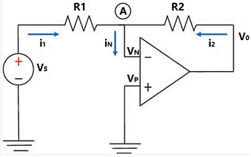
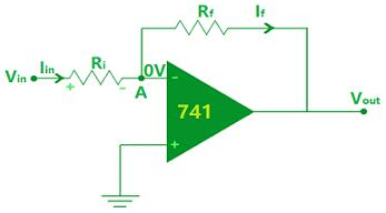
Figure 2. Inverting Operational Amplifier Circuit
2. Operational Parameters
To effectively utilize operational amplifiers in circuits, it is essential to have a grasp of their internal parameters. The following are technical specifications closely related to operational amplifiers:
Unit Gain Bandwidth
Definition: Under the condition that the operational amplifier's closed-loop gain is set to 1x, an equal-amplitude sine wave signal is input to the operational amplifier's input terminal. The closed-loop voltage gain of the operational amplifier is reduced by 3dB (or equivalent to 0.707 times the operational amplifier's input signal), meaning the frequency at which the output signal drops by -3dB is known as the unity-gain bandwidth. This is a crucial parameter. For sine wave amplification with small signals, the unity-gain bandwidth is equal to the product of the input signal frequency and the gain at that frequency. In other words, when the frequency and gain of the signal to be processed are known, the unity-gain bandwidth (gain bandwidth = amplification factor * signal frequency) can be calculated to select an appropriate operational amplifier.
For small signals, unit gain bandwidth, also known as gain-bandwidth product, roughly indicates the operational amplifier's ability to process signal frequencies. For instance, if an op-amp has a gain-bandwidth of 1MHz and the actual closed-loop gain is 100, the theoretical frequency of processing small signals would be 1MHz/100 = 10kHz.
For the bandwidth of a large signal, i.e., the power bandwidth, the impact of the slew rate (SR), measured in V/us, is a primary factor. At this point, the power bandwidth, calculated as FPBW = SR / (2πVp-p), must be considered alongside the gain bandwidth when designing the circuit.
For DC signals, bandwidth concerns are generally not considered; precision and interference are the primary factors.
When the amplifier's gain is set to n times, it does not mean that all input signals are amplified by n times. As the signal frequency increases, the amplification capability decreases.
Open Bandwidth
The open-loop bandwidth is defined as the frequency at which the voltage gain from the output of an operational amplifier drops 3dB below its DC gain when an equal-amplitude sine wave signal of very small magnitude is applied to the input. This is used for processing very small signals.
Conversion Rate SR
Closing the feedback loop of an operational amplifier (op-amp), input a large signal (including step signals) to its input terminal, and measure the op-amp's output rise rate, which is referred to as SR. Since the input stage of the op-amp switches during the conversion process, the feedback loop does not function, meaning the conversion rate is independent of the closed-loop gain. Conversion rate is a critical indicator for large signal processing. For general op-amps, the slew rate SR is <= 10 V/μs. Currently, high-speed op-amps can achieve a conversion rate of up to 6000 V/μs. The higher the SR, the better the op-amp's response to high-speed input signals. A larger signal amplitude and higher frequency result in a higher SR.
Full Power Bandwidth
Under rated load, with the operational amplifier's closed-loop gain set at 1x, a sinusoidal large signal of equal amplitude is input to the amplifier's input terminal, causing the output frequency of the amplifier to reach a signal with permissible distortion. This frequency is limited by the operational amplifier's conversion rate (SR). The full-power bandwidth is approximately calculated by the formula SR / (2πVop) (where Vop is the peak output amplitude of the operational amplifier). It is a very important specification for selecting operational amplifiers in large signal processing.
Set Date
Under rated load conditions, with the operational amplifier's closed-loop gain set at 1x, the time required for the output to increase from 0 to a specified value upon the input of a step signal. Due to the step signal input, the output signal will exhibit some oscillation after reaching the specified value, which is referred to as the settling time. At this point, the settling time + rise time equals the settling time. The settling time varies significantly with different output accuracies; the higher the accuracy, the longer the settling time.
Equivalent Input Noise Voltage
The term refers to any alternating current random interference voltage generated at the output of an operational amplifier (op-amp) with good shielding and no signal input. When this noise voltage is converted to the input of the op-amp, it is known as the input noise voltage of the op-amp (sometimes expressed as noise current). For broadband noise, the root mean square (RMS) value of the input noise voltage of a typical op-amp is approximately 10 to 20 μV. This value usually corresponds to a specific frequency band.
Output Impedance
It refers to the ratio of voltage change to the corresponding current change when a signal voltage is applied to the output of an operational amplifier operating in the linear region. At low frequencies, it simply refers to the output resistance of the operational amplifier.
Common-mode input resistance
The ratio of the change in common-mode input voltage to the corresponding change in input current when the two input terminals of an operational amplifier receive the same signal. At low frequencies, it manifests as common-mode resistance. Generally, the common-mode input impedance of an operational amplifier is much higher than the differential input impedance, with typical values exceeding 108Ω.
Common Mode Rejection Ratio
As defined in differential amplification circuits, it is the ratio of differential voltage gain to common-mode voltage gain, typically expressed in decibels. It is a parameter that measures the symmetry of the input differential amplifier and the integrated operational amplifier's ability to suppress common-mode interference signals. The higher the value, the better.
Power Suppression Ratio
The power supply rejection ratio (PSRR) is defined as the rate of change of the operational amplifier's input offset voltage within the linear region with respect to the power supply voltage. The PSRR indicates the impact of power supply variations on the amplifier's output. Currently, the PSRR is only around 80dB. Therefore, careful power supply setup for the operational amplifier is required when used for low-level signal processing in DC or analog amplification applications. Of course, operational amplifiers with high common-mode rejection ratio (CMRR) can compensate for some of the PSRR. Additionally, when using dual power supplies, the PSRR of the positive and negative power supplies may differ.
Differential Mode Input Resistance
The ratio of the change in voltage at the two input terminals to the corresponding change in input current when an operational amplifier operates in the linear region. Differential input impedance includes input resistance and input capacitance, referring only to the input resistance at low frequencies. Generally, product specifications only provide the input resistance. For operational amplifiers using bipolar junction transistors as the input stage, the input resistance is not greater than 10MΩ; for operational amplifiers using field-effect transistors as the input stage, the input resistance is generally greater than 10^9Ω.
Input Voltage Mismatch
When the input voltage is zero, the output voltage divided by the voltage gain, plus the negative sign, converts to the input offset voltage. It is the compensation voltage applied to the input when the output voltage is zero. The input offset voltage actually reflects the symmetry of the operational amplifier's internal circuit. The better the symmetry, the smaller the input offset voltage. The input offset voltage is a very important indicator of the operational amplifier, especially when it is a precision operational amplifier or used for DC amplification.
Input offset voltage is related to manufacturing processes. When an operational amplifier is implemented using bipolar technology (i.e., standard silicon technology), it is typically between ±1 and 10 mV. Using a field-effect transistor as the input stage can increase this value. For precision operational amplifiers, it is generally below 1 mV. The smaller the input offset voltage, the smaller the intermediate zero bias during DC amplification, and the easier it is to handle. Therefore, it is an important specification for precision operational amplifiers.
Input失调 voltage drift
Within the specified operating temperature range, it is the ratio of the input offset voltage change to the temperature change. It essentially complements the input offset voltage, facilitating the calculation of drift in amplifier circuits due to temperature variations within the given operating range. It is a key indicator of the impact of temperature on operational amplifiers. Generally, it is around (10~30) uV/C (degrees Celsius), with high-quality options being less than 0.5 uV/C.
Input Current Imbalance
It is defined as the difference in the base current of the differential input stage when the operational amplifier's output DC voltage is zero. It is used to characterize the degree of asymmetry in differential input current. The better the symmetry, the smaller the input offset current. Input offset current is a very important indicator for operational amplifiers, especially for precision operational amplifiers or DC amplifiers. The input offset current is approximately one to one-tenth of the input bias current. It has a significant impact on small-signal precision amplification or DC amplification, particularly when using large resistors externally in operational amplifiers. The effect of input offset current on precision may exceed that of input offset voltage. The smaller the input offset current, the smaller the intermediate zero bias during DC amplification, making it easier to handle. Therefore, it is an important indicator for precision operational amplifiers.
Input失调 current temperature drift
The ratio of the change in input失调 current to the change in temperature within the specified operating temperature range. It refers to the temperature coefficient within the specified operating range and is an important indicator for measuring the impact of temperature on operational amplifiers. Typically, it is around (1-50) nA/C, with high-quality ones being around pA/C. This value is only provided in precise operational amplifier parameters and should be noted when dealing with DC signal processing or small signal processing. Signal processing.
Input Bias Current
Defined as the average bias current of the two input terminals when the operational amplifier's output DC voltage is zero, in other words, it is the average current flowing into the input terminals when the operational amplifier is operating in the active state. Linear region. The input bias current has a significant impact on areas requiring input impedance, such as high-impedance signal amplification and integration circuits. The input bias current is somewhat related to the manufacturing process. If a field-effect transistor is used as the input stage, the input bias current is generally lower than 1nA. It is commonly used to measure the input current of a differential amplifier pair.
Differential Input Voltage
It is the voltage that the two input terminals of an operational amplifier can withstand. When exceeded, it will cause the differential transistor to experience reverse breakdown. The NPN transistors, made using planar technology, have a Vidmax of about 5V, while the Vidmax of horizontal PNP transistors can reach over 30V.
Common Mode Input Voltage
It is the common-mode input voltage range allowed under the normal operating conditions of the operational amplifier. When the differential input pair is saturated, the amplifier loses common-mode rejection capability. This issue should be noted during circuit usage in the presence of interference.
Peak-to-peak voltage output
Operating in the linear region, under specified loads, the voltage amplitude that an operational amplifier (op-amp) can output when powered by a large power supply is referred to as the output voltage amplitude. For general-purpose op-amps, the peak-to-peak output voltage is typically greater than ±10V but less than the supply voltage, due to the design of the output stage. Modern low-voltage op-amps have a specially treated output stage, with the peak-to-peak voltage close to the supply voltage within 50mV, hence termed as full-scale output op-amps or rail-to-rail op-amps. It's important to note that the peak-to-peak output voltage of the op-amp is load-dependent, varying with different loads; the positive and negative output voltage swings of the operational amplifier may not be identical.
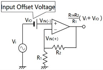
Figure 3. Input Offset Voltage of the Operational Amplifier
III. Application Matters
1) Single-supply op-amps must be biased with DC, otherwise they will not operate properly. For virtual ground designs, in addition to the DC potential, attention must be paid to voltage regulation (using a reference voltage chip), and low-impedance AC decoupling must be ensured, i.e., parallel decoupling at least 10uF for low frequencies, and less than 0.1uF for high frequencies.
The input of the phase amplifier must be biased to ground as a DC path.
3) Standard operational amplifiers cannot directly drive capacitive loads. If necessary, a capacitor for phase compensation or a series resistor at the output must be used before connecting the load.
4) For the operational amplifier input of external interfaces, a TVS diode must be connected in parallel with the positive and negative input pins to prevent the op-amp from polarity reversal due to excessive input voltage signal, which could generate parasitic false signals.
5) For amplifier circuits with gain greater than 10 times, pay attention to controlling the bandwidth gain of the operational amplifier to prevent device self-oscillation.
6) The amplifier output requires protection via switching diodes to the power supply and ground, especially when connected to inductive loads.
7) When processing multiple signals with multiple operational amplifiers, it's crucial to prevent the transient changes of one signal from causing crosstalk to another. Therefore, it is recommended not to use a single op-amp to handle multiple signals.
8) Most operational amplifier (op-amp) chips are ESD-sensitive devices; extra caution is required during use.
9) Unused op-amp pins (extra channels within multiple op-amps) should not be left floating, grounded, or connected to the positive and negative power supplies. It is recommended to connect them as followers (output connected to inverting input), with the non-inverting input connected to the potential between the power rails (ground in a dual-power supply system or any suitable point in the circuit). They can also serve as buffer amplifiers and can be added to the system's minor-impact positions.