
MOSFETs inherently possess three parasitic capacitances: Cgs, Cgd, and Cds. This is reflected in the datasheet of MOSFETs, where these are often replaced by the parameters Ciss, Coss, and Crss. The Miller effect present in MOSFETs and the need for series resistors between the GS terminals both originate from these three parasitic capacitances.
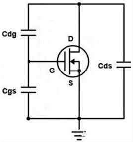
Internal MOSFET parasitic capacitance illustration

Parasitic Capacitance Parameters
Miller Effect in MOS tubes
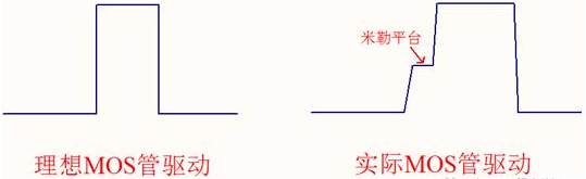
Ideal vs. Reality of MOSFET Drivers
The ideal drive waveform for a MOSFET should be a square wave, and once the Cgs reaches the threshold voltage, the MOSFET enters a saturated conduction state. However, in the process of driving the gate of a MOSFET, a Miller plateau is present. The Miller plateau is a typical sign that the MOSFET is in the "linear region," leading to significant conduction losses. Thus, the Miller effect is an objectively existing phenomenon that is detrimental to the circuit, and it must be considered during circuit design.
The Detailed Process of Miller Platform Formation:
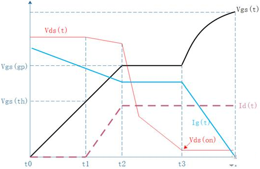
MOSFET turn-on process
Breakdown the MOSFET turn-on time:
t0→t1: When the voltage across the GS terminals of the MOSFET reaches the threshold voltage Vgs(th) (which can be understood as charging the Cgs), the MOSFET begins to conduct, and before this, the MOSFET is in the cutoff region.
As Vgs continues to increase, Id begins to rise, and Vds starts to decrease. At this point, the MOSFET operates in the saturation region (How do you determine if it's in the saturation region? You can directly deduce from the formula: Vds > Vgs - Vth. Analyze the Vds-Id output characteristic curve in reverse). Id is mainly determined by Vgs, and during this process, Vds will slightly decrease, primarily due to the △I causing a more significant parasitic inductive reactance, leading to voltage drops.
t2→t3: After Vgs increases to a certain extent, the Miller effect occurs, and Id has reached saturation. At this point, Vgs will remain constant for a period of time without further increase, while Vds continues to decrease, charging Cgd. It is precisely because Cgd needs to be charged that the voltage change between Cgs is relatively small (when the MOSFET is turned on, Vd > Vg, Cdg discharges first through the MOSFET and then is recharged in the opposite direction, taking away the charging current intended for Cgs, resulting in the Vgs plateau).
t3→t4: As Vgs continues to rise, the device enters the variable resistance region, DS conducts, and Vds decreases. (The Miller plateau, by limiting the increase of Vgs, also limits the decrease of the conductance resistance, thereby limiting the decrease of Vds, which prevents the MOSFET from quickly entering the switching state.)
2. The resistive function between the Gate (G) and Source (S) terminals of a MOS tube
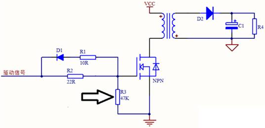
Inverting Power Supply Schematic: R3 is the GS resistor
To demonstrate the importance of the GS resistance with a simple experiment: Take a MOSFET, leave its gate (G) unconnected, and apply voltage across the drain-source (DS). Results show that when the input voltage is only 30 to 40 volts, the MOSFET's DS will conduct directly, which could potentially damage the device if not limited. It would be expected that without drive, the MOSFET should not conduct. However, due to the parasitic capacitance of the MOSFET, when voltage is applied across DS, it charges Cgs through Cdg, raising the gate voltage until the MOSFET conducts. (If a transformer drive is used, the transformer winding can act as a discharge, so even without GS resistance, the tube will not conduct on its own when there is no drive.)
Paralleling a resistor (with a value of a few K to several tens of K) between the GS terminals can effectively ensure the normal operation of the MOSFET. Firstly, when the gate is floating, the voltage between the DS terminals will not cause the MOSFET to conduct and be damaged. Additionally, without drive, it can clamp the gate of the MOSFET to a low level, preventing false operation and ensuring reliable switching.
